A related question is a question created from another question. When the related question is created, it will be automatically linked to the original question.
If you have a related question, please click the "Ask a related question" button in the top right corner. The newly created question will be automatically linked to this question.
Can you please show an schematic to clarify the voltage supply connections, bypass capacitors and output load conditions. Please also show the voltage applied at the non-inverting input, and the voltage measured at the output of each amplifier in the schematic. How many amplifiers show this issue? Is the OPA4197 soldered on a PCB board?
The Operational amplifier's output can only swing within a few 10-100's of millivolts from the supply rails.
The output swing of the amplifier is limited to 5 to 25mV from the rail supplies with no load (at room temperature). The output swing range depends on the output load and temperature conditions. In your case, since you have shorted the (V+) supply and the non-inverting input (+IN), using the amplifier in the buffer configuration, the output of the amplifier will be around 5 to 500mV below the (V+) rail supply depending on the temperature and the load condition. In this circuit, you are placing the amplifier outside its linear range of operation since you are exceeding the output swing range of the amplifier.
Please see the "Voltage Output Swing" specification and "Open Loop Gain (AOL)" specifications on the Electrical Characteristics table on page 9-10 of the OPA4197 datasheet. The conservative approach is to design the buffer circuit so that the amplifier output is always within ~300mV from the positive and negative rail supplies (or 600mV depending on the load condition). This will ensure the amplifier is well inside its linear range of operation.
If you wish to learn more about the input/output voltage range specifications of Operational amplifiers please check out the PLABs video tutorial below.
3. TI Precision Labs - Op Amps: Input and Output Limitations
Rail-to rail output amplifiers are only able to swing close to the supply rails. In the case of the OPA4197, the output of the amplifier can reach within 430mV of the positive supply rail when using a 2kOhm load. In your circuit, the input impedance of the second stage amplifier is loading the output of the amplifier, and therefore the output of the buffer is only expected to reach within 430mV of the supply rail as specified on the device datasheet.
If you need a op-amp buffer to amplify a 16-V signal, you will need to provide a supply that exceeds the input signal by some headroom. Looking at the AOL specification of the OPA4197, a conservative approach would be to use a +16.6V supply to amplify a 16-V input signal.
Rail-to rail output amplifiers are only able to swing close to the supply rails. In the case of the OPA4197, the output of the amplifier can reach within 430mV of the positive supply rail when using a 2kOhm load. In your circuit,
An output current load graph should indicate how far from rail it can sustain typical current loads? How is 430mV below VCC considered Rail to Rail operation in unity gain configurations? The 2k into the input drive is loading the output, Tina model confirms loading?
Should not the output slew be able to drive an input (of the same IC) "without any resistor" maintain Rail-to-Rail current load specification? How can the input quiescent current, ever load the output via 2k series resistor?
I don't even see a 2k only 1k feed back resistors. Perhaps B-total divider is current limiting or starving VCC rail? Hard to tell what is what in the schematic without voltage indicators...
The OPA197 output swing performance is similar to other rail-to-rail output swing amplifiers in the market and consistent with rail-to-rail output amplifiers from other manufacturers as well.
The typical specification for output swing is 5-mV to the positive rail supply at room temperature with no load (25mV max). When applying a 2kOhm load, the output swing typical specification is 430mV to the supply rail at room temperature (500mV max).
The output swing characteristic changes depending on load and temperature conditions. Please refer to the "Voltage Output Swing" and "Open Loop Gain" specifications on the Electrical Characteristics table of the OPAx197 datasheet. Also, check Figure 15, "Output Voltage Swing Specification from Positive Power Supply vs Output Current". The conservative approach is to design operational amplifier circuits using the AOL (open-loop gain) specification. For example, the output is allowed to swing 0.6V from the rail supplies when using a 2kOhm load.
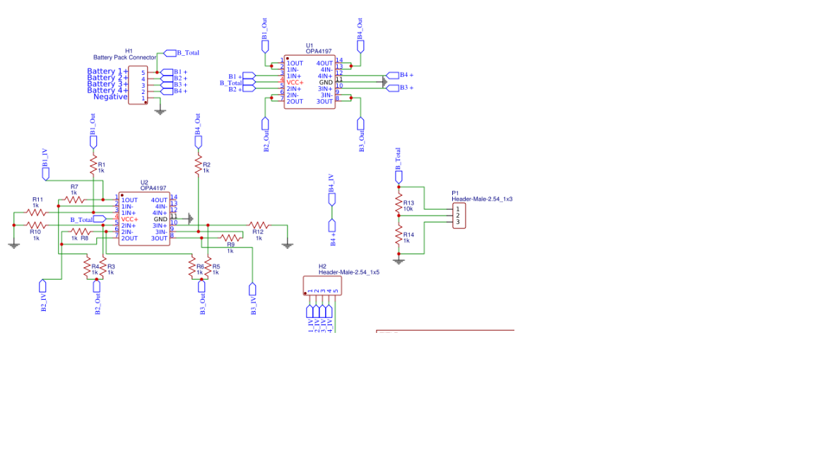
If I interpreted the post above correctly: all 4 channels of U1 (OPA4197) are setup in the buffer configuration, and all 4 channels of U2 (OPA4197) are configured in a difference amplifier configuration using 1kOhm resistors. In this circuit, OUT1 of U1 connects to (1IN+) of U2 (also OPA4197).. OUT1 of U1 sees a 1kOhm+1kOhm load to ground since is driving the difference amplifier on U2.
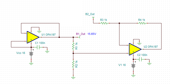
If I understood the text on the post description above, Pin4 VCC+ of U1 and PIN3 (1IN+) are shorted together to +16V, placing 1OUT buffer on the positive rail. In this condition, buffer1 of amplifier U1 can not swing to the positive rail since it is well outside is linear range of operation, with its input driven to the rail supply, and its output loaded with a 2kOhm load.
Please see the customer schematic below, and TINA simulations showing the output can only swing around ~15.65V on this condition.
The conservative approach is to design operational amplifier circuits using the AOL (open-loop gain) specification, where the output is allowed to swing 0.6V from the rail supplies when using a 2-kOhm load.
Please use a higher voltage supply (>16.6V or so) to allow headroom for the buffer amplifier to drive the 2kOhm loaded output to 16-V and remain well in its linear range of operation. In other words, the VCC+ supply needs to be 0.6V higher than the input signal you are required to buffer in this circuit.
The typical specification for output swing is 5-mV to the positive rail supply at room temperature with no load (25mV max). When applying a 2kOhm load, the output swing typical specification is 430mV to the supply rail at room temperature (500mV max).
Again hardly rail to rail operation (5mV No load) is like saying " If you don't have the output connected to anything, rail to rail can be achieved." My point was as you have stated to refer to current load graphs. TI should add the word NEAR in front of the word Rail as it is no were close to Full rail to rail operation but only under no output load condition is a disingenuous datasheet description. Perhaps the industry regulation agency/s have become complacent letting marketing hype to fly under the radar!
Note System is battery powered monitor of sorts may not be possible to raise VCC 0.6v. Perhaps changing R1/R2 (Tina) value to match load graphs Fig.15 is a better WA.
One possible option is to increase the resistance values of the difference amplifier to 100kOhm or 1MOhm. If the battery application is able to handle the input 1-MOhm input impedance of the difference amplifier, you may consider connecting the difference amplifier directly without a buffer stage.
In general, linear operational amplifiers will have an output swing that is limited below the rail supplies due to their output stage architecture; where the output swing characteristic will change with load. Unfortunately, the term 'rail-to-rail' output on operational amplifiers has been used for many years all across the industry.
Please find below the Precision Labs session that discusses in good detail the output stage limitations of operational amplifiers and a EDN article that also discusses the topic.
Thank you and Regards,
Luis
TI Precision Labs session
3.4 TI Precision Labs - Op Amps: Input and Output Limitations 3
You say schematic pin 3(+IN) & pin 4(VCC) are (shorted) -- then show B1+ from battery seems very odd. Perhaps battery input +4.2v on pin 3=(B1+) must NOT be shorted together with pin 4=(VCC) on PCB since VCC = +16v will make battery the same voltage?
As we discussed on the posts above, eliminating the buffer stage and directly connecting the OPAx197 in a difference amplifier configuration, and scaling the difference amplifier resistors properly will allow you to measure a higher range of input signals.
If you wish us to suggest a circuit, to avoid any confusion, please provide a detailed schematic that clearly shows the voltage supplies used, and clearly displays all the battery voltage level ranges that will be required to be measured in this application.
I have not any external power I am just using four lithium battery connected in series (pack voltage is 16.8) and I want to measure that voltage of each cell.
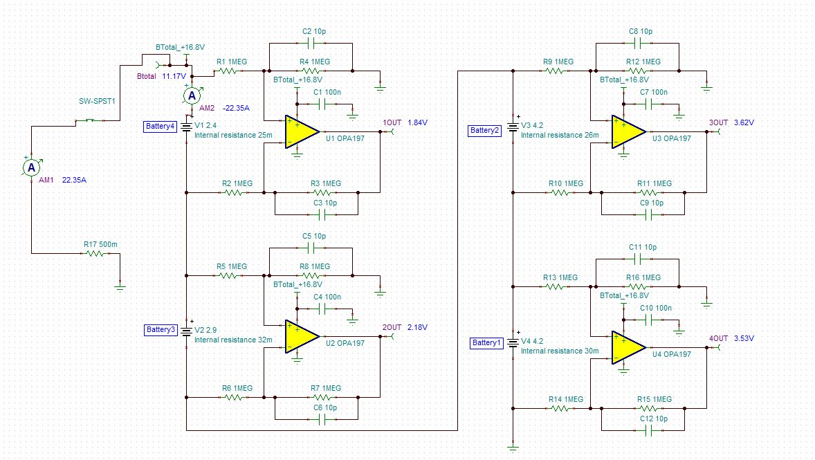
One suggestion is to eliminate the buffer stage, and configure the four channels of OPA4197 in a difference amplifier configuration using 10MOhm (or 1MOhm) resistors as shown below.
The 4 x 4.2V battery cells produce +16.8V, and this voltage is used as a power supply for the OPA4197. Each cell is measured producing 4.2V at the output of each OPAx197 channel. Please see figure and attached simulation.
Yes, since you have modeled a 25mOhm to 32mOhm series resistance on the battery cells on the simulation, a voltage drop occurs on the battery as you draw current.
For example, on the V1 cell, the voltage drop due to the battery resistance is 25mOhm*22.35A = 0.558 V.
therefore the voltage across the cell V1 is approximately 2.4V - 0.558-V = ~1.842-V as expected.
The resistor values used on the difference amplifier set the overall input impedance of the amplifier:
- The resistor values must be large compared to the output impedance of your source. In a battery measurement application, the battery output impedance is very low, on the 10's to 100's of milli-ohms, so you may reduce the impedance of the difference amplifier without adding significant error due to the input impedance. However, the trade-off of reducing the resistor values is that your difference amplifier will consume more current at its inputs.
- Using large resistors will add noise on the circuit, and could also degrade phase margin which could potentially cause stability issues. Avoid placing capacitive loads at the output of the difference amplifier to mitigate the risk of stability issues. One thing you can do to reduce noise and improve phase margin of the difference amplifier is add capacitors on the feedback and reference resistor of the difference amplifier as shown on the previous example above.
- You also have to consider the effect of the input offset current of the operational amplifier when using large resistors. The OPA197 is a CMOS amplifier with 2pA of bias current at room temperature; but could be as high as 2nA at 125C (please refer to the Electrical Characteristics table on page 7, and figure 13 of the OPA197 datasheet). If your application requires to operate at hot temperatures, you may consider using 1-MOhm (or smaller resistor values depending on your error budget) to avoid errors due to the input offset current of the amplifier interacting with the resistor
Below is a difference amplifier circuit design example from the Analog Circuits Cookbook collection. Our Analog Engineer’s Circuit Cookbooks are a compilation of sub-circuit designs in an easy-to-use e-book. Each circuit within the e-book includes step-by-step instructions, basic formulas, schematic diagrams and SPICE simulations