This thread has been locked.
If you have a related question, please click the "Ask a related question" button in the top right corner. The newly created question will be automatically linked to this question.
Hello,
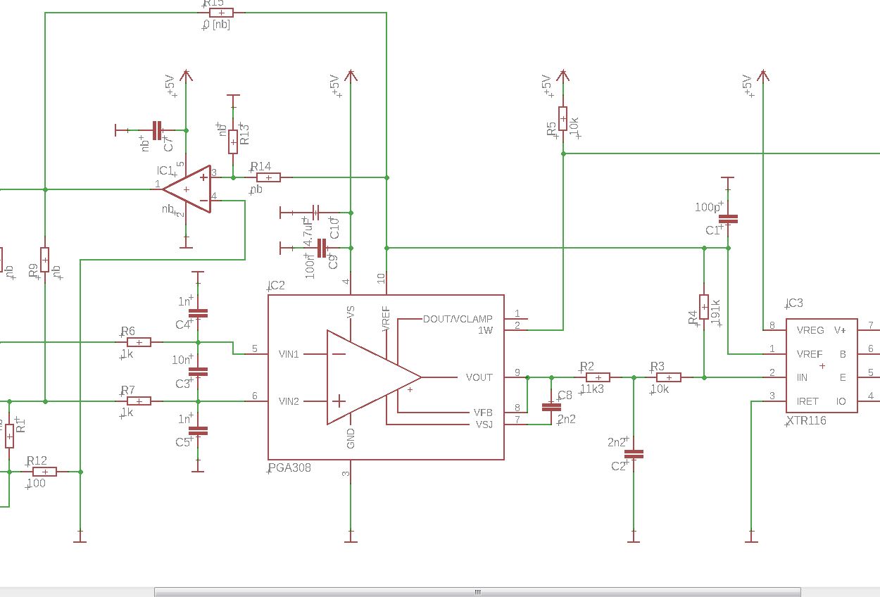
I use the PGA308 in an application, I want to calibrate it first with ram values and then write the values into the otp registers. My Vref is 4,096V
This is how I want to do it:
At Point 3. I recognize that even if I change the ram registers my Vout doesn’t change.
At Point 11. I recognize that I can’t write to OTP, if I read the values nothing is written there.
This is my circuit diagram:
What is my mistake?
Hi Tobias,
You have mentioned that you have confirmed that the OTP's are not being programmed.
-Are you using the PGA308EVM USB DAQ controller to program your PGA308 Custom board or are you using a different controller/different software?
- When programming the RAM registers, are you able to confirm that the RAM registers are programmed? In other words, are you able to read and confirm the RAM register contents after writing them?
If you are unable to read/write the RAM registers, have you confirm/checked the PGA308 1W communication with an external oscilloscope?
Thank you and Regards,
Luis
Hi Luis,
yes the OTP's are not programmed before.
I can write and read the RAM Values without any problem.
I use an own one wire adapter with a standard terminal software. Of course, i checked the signal on an external oscilloscope and it's looking pretty good.
Hi Tobias,
1) The schematic shows the DOUT/VCLAMP is left floating or disconnected... The DOUT SEL bit (CFG2 Register [D8]) sets the DOUT/VCLAMP pin as either a digital output function (DOUT SEL = 1) or as a VCLAMP function (DOUT SEL = 0). Can you please confirm 'DOUT SEL bit is set to '1'? In VCLAMP Mode, the Amplifier output, VOUT, is limited to the voltage applied to the DOUT/VCLAMP pin, and this may be clampling/limiting the PGA308 output.
2) The XTR116 recommends a 2.2uF to 22uF bypass capacitor at the XTR116 regulator pin. (Please refer to figure 5 of the XTR116 datasheet). Can you verify you have a minimum 2.2uF bypass capacitor at the XTR116 regulator?
3) The Vs supply must exceed 4.5-V to ensure reliable programming of the OTP. The schematic shows that the PGA308 is powered by the VREG of the XTR116, which is expected to be 5-V; which should work when it has the bypass capacitor... Can you please quickly verify with external meter that the voltage between pin (3) GND and pin (4) Vs is around 5-V (or exceeding 4.5V)?
4) What is the differential input voltage at sensor low (voltage across Vin1 and Vin2) when measuring with an external meter? What is the voltage at PGA308 output (PGA308 pin 9) at sensor low?
5) What is the differential input voltage at sensor high (voltage across Vin1 and Vin2) with external meter? What is the voltage at PGA308 output (PGA308 pin 9) at sensor high?
6) Is it possible to provide the complete schematic. (please let me know if you prefer to be contacted via email).
Thank you and Best Regards,
Luis Chioye
1. DOUT is always set now. No change of the Output
2. Capacitor is at the regulator pin
3. The Supply has stable 5V
4. Diff min 77mV, diff max 666mV, output low 25mV output high 26mV
5. Of course i can show u the complete shematic but only via email.
Its possible to write to top now, didnt set the otp enable bit first.
Hi Tobias,
Thank you for the confirmation that its now possible to write the OTP's. If I understood the last post correctly, you are now setting the 'DOUT SEL' bit to '1' with DOUT/VCLAMP set as a digital output function. If this is the case, DOUT/VCLAMP can be allowed to float and should not clamp the output of the PGA308; otherwise you would have to connect VCLAMP to VS (pin 4).
The XTR116 Reference pin requires a compensation capacitor with an Rcomp (or RISO) resistor as shown on the figure below, which does not show on the schematic excerpt on the post. Can you please confirm if you have one of this compensation schemes on the hardware? Please confirm with external meter the reference voltage is 4.096V at the PGA309 reference input (pin 10) with respect to the GND (pin 3)?
Thank you and Best Regards,
Luis
XTR116 Reference pin compensation capacitor and RISO or RCOMP resistor.
Hi Tobias,
Just wanted to follow-up, please let me know if the issue with the PGA308 output not changing with input voltage persists after adding the XTR116 reference pin compensation above and checking the reference pin voltage with an external meter.
Thank you and Best Regards,
Luis
Hello Luis,
my mistake was not to connect the metall plate on the ground of the pga with the ground of the pcb.
Now everything works fine