This thread has been locked.
If you have a related question, please click the "Ask a related question" button in the top right corner. The newly created question will be automatically linked to this question.
Hi officer,
I am writing to enquire about one problem I met on '2.2 TI Precision Labs - Op Amps: Vos and Ib - Lab'.
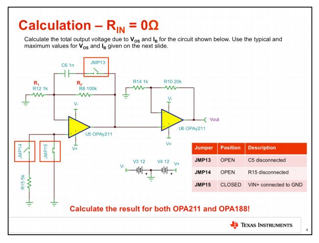
the screenshot below shows the schematic.
And at 03:06, it shows a Req calculation in pic below:
I am confused by why 'Req = Rf R1 /(Rf + R1).'
can anyone please help on this?
thanks,
Jim
Hey Jim,
That looks like an error to me. If the V+ node is grounded, the output error due to inverting Ib is -Ib*Rf ( often Ib is unipolar. The OPA211 spec table looks be in error also shows a +/-200nA whereas the schematic shows an NPN differential input - unless there is bias current cancellation not being shown, the input bias current is unipolar into the device - that give an output error showing a positive shift (From Vos*noise gain error) in the Vo as +Ib*Rf. The Rf||Rg calculation in the video is heading towards a bias current cancellation where you make the DC source R on the V+ input equal to that. That will then reduce the DC output error due to input bias currents of that first stage to +/-Ios*Rf where Ios is almost always bipolar mismatch currents.
Hi Michael,
THANKS for your reply.
I agree with your first part of explanation.
However I do not understand the second part
'The Rf||Rg calculation in the video is heading towards a bias current cancellation where you make the DC source R on the V+ input equal to that. That will then reduce the DC output error due to input bias currents of that first stage to +/-Ios*Rf where Ios is almost always bipolar mismatch currents. '
Did you mean that adding a R = Rf||Rg between V+ and ground will reduce the DC output error to +/-Ios*Rf ?
Isn't that first stage bias current error, Vout-ib = +/-Ios*Rf when the V+ is connected to ground directly?
thanks,
Jim.
Yes, to get bias current error cancellation, set the R = Rf||Rg between V+ and ground will reduce the DC output error to +/-Ios*Rf.
If you connect V+ to gnd directly, there is no contribution to output error for the IB+ term and you just get an -Ib*Rf quite a lot higher (usually, for bipolar inputs) than Ios*Rf.
More detail Jim,
I did look closer at the spec table and this device almost certainly has a bias cancellation at the inputs. So the Ib term can indeed be bipolar - you can tell that by the much higher than expected current noise term vs the typical Ib term. Normally closely related by a simple equation, but since the current noise far exceeds that calculation, must have another current coming into those input pins to try and cancel the input base current,
One tradeoff there is you do get a much lower nominal input bias current but your Ios is not stepped down as much as simpler input stages. The equivalent schematic is apparently simplified.
Hello Jim,
"I am confused by why 'Req = Rf R1 /(Rf + R1)."
The OPA211, or any Op amp in this circuit configuration has its inverting input the summing node connected to one node of the R1 input resistor and one node of the the RF feedback resistor. The other end of R1 connects to ground (~zero impedance) and the other end of RF connects to the Op amp output - a very low impedance also. So as far as the impedance that the inverting input sees it is R1 || RF, or Req = (RF R1) / (RF + R1).
The OPA211 inverting input bias current is provided by these two resistors as the sum of the current through them. How much R1 and RF each provides towards the necessary input bias current is a function of the voltage offset of the Op amp, the circuit's closed-loop noise gain, and the sign of the output referred voltage offset.
Regards, Thomas
Precision Amplifiers Applications Engineering
Huh?? I have never seen that before - if you sum output DC errors through superposition, the inverting bias current (since V- is at zero volts) goes only through the Rf resistor as a gain element to the output. You could perhaps model it as a voltage on the inverting node that is Ib *(Rf||R1) that then has a voltage gain to the output of (Rf+R1)/R1 that, if you multiply that out, gets you back to a gain of Rf - or you could just use Rf as the gain.
But really, if you are doing superposition and the V+ input is grounded with no Vos error, the inverting node is also at ground - the approach shown in the video will not show up in sim
That is correct. OPA211 does have the input bias cancellation circuitry (as indicated in the datasheet by +/- sign in front of IB) and for that reason you may NOT attempt to cancel IB related error by adding a parallel combination of R1||Rf in series with the non-inverting input. Doing so, may instead double the error in case +IB and –IB currents happen to flow in the opposite direction).
If you assume the inherent Vos=0, the IB generated input voltage error is Vin_error [IB] = IB*(Rf||Rin) = IB*R1*Rf/(R1+Rf) but after referencing it to the output, Vout_error [IB] = Vin_error*Gain = -[IB*R1*Rf/(R1+Rf)]*[(R1+Rf)/R1] and therefore, Vout_error [IB] = -IB*Rf, as expected.
Hello Thomas,
Thank you so much for that explanation. Now I understand where that Req comes from.
Can I have your opinion on the calculations after that Req in the lecture video?
In the lecture,
Vout_error = G1G2 (Vos+Vib). If we separate the error Vout_error_ib caused by the Ib from the error Vout_error_Vos caused by Vos.
Vout_error_ib = G1 x G2 X Vib = (R1+Rf)/R1 x G2 x ib x Req = (R1+Rf)/R1 x G2 x ib x Rf R1/(Rf +R1) = G2 x ib x Rf.
My calculations:
ib_U5, bias current of the first OPA211 (U5 in the schematic below).
ib_U6, bias current of the first OPA211 (U6 in the schematic below).
Vout_error_ib = ib_U5 x Req x G1 x G2 + ib_U6 x Req2 x G2 = ib_U5 x Rf R1/(Rf +R1) x (R1+Rf)/R1 x G2 + ib_U6 x Req2 x G2
= ib_U5 x Rf x (R10+R14)/R14 + ib_U6 x R10*R14/(R10+R14) x (R10+R14)/R14
= ib_U5 x Rf x (R10+R14)/R14 + ib_U6 x R10
= ib_U5 x Rf x G2 + ib_U6 x R10
It seems that the lecturer has omitted 'ib_U6 x R10', error brought by the bias current of the second OPA211.
Can you please correct me if I was wrong?
Thanks,
Jim.
Hi Marek,
Thanks for your reply.
I think that Vout_error [IB] = -IB*Rf is the error to the output of the first stage opa211.
I am confused by how the lecturer calculated that total IB error.
To get the total IB error to the final output (error output of the second opa211), i think
Vout_error [IB] _ total = -IB_U5 * Rf *G2 + IB_U6 *R10
ib_U5, bias current of the first OPA211 (U5 in the schematic below).
ib_U6, bias current of the first OPA211 (U6 in the schematic below).
G2, closed loop gain of second opa211
R10, feedback resistor of second opa211.
However, in the lecture, the lecturer wrote:
Vout_error = G1G2 (Vos+Vib). If we separate the error Vout_error_ib caused by the Ib from the error Vout_error_Vos caused by Vos.
Vout_error_ib = G1 x G2 X Vib = (R1+Rf)/R1 x G2 x ib x Req = (R1+Rf)/R1 x G2 x ib x Rf R1/(Rf +R1) = G2 x ib x Rf.
It seems that the lecturer has omitted 'ib_U6 x R10', error brought by the bias current of the second OPA211.
can you please let me know if I was right or wrong?
thanks.
Thanks,
Jim.
Yes Jim, the precision labs is confusing, the new model shows this if I just run a DC simulation.
So the model has 30.56uV input offset, that gets to the output times 2 or about 61uV - taking that from the output 411uV leaves 350uV to explain. That is 350uV/10k = 35nA going into the V-node. both of these make sense relative to the typical data sheet numbers. The bias current does not move the V- node. If we thought that it did, that 35nA times 5k would be a -175uV on the V- nodes and we do not see that since the loop holds the V-node at ground + Vos.
Jim,
Yes, that's correct: Vout_error [IB] = -IB*Rf is the IB related error at the output of the first stage. Even though, as you correctly pointed out, the total IB related error at the output of second stage is: Vout_error [IB] _ total = -IB_U5 * Rf *G2 +/- IB_U6 *R10, the second term (IB_U6*R10) contribution is 101 times smaller than the error of the first stage (it's NOT gained up by 101) and for that reason it has been neglected in TI Precision Lab lecture.
Micheal,
In total error consideration, you must treat each contribution like Vos and IB error separately – thus if you calculated Vos related error, you assume IB=0 and in case of calculating IB related error you assume Vos=0. Therefore, as you correctly pointed out, according to the OPA211 model, the inherent Vos is 30.56uV so by reflecting it to the output, its contribution is 61uV. This leaves 350uV Vout error to account for, which can be done either by directly calculating the output error as you have done (IB*RF=35nA*10k - no current flowing thru R1 because Vos is assumed to be zero) or calculating the input referred IB error: Vos_IB = IB*RF||R1) = 35nA*10k||10k) = 175uV and then reflecting it to the output by multiplying it by the close-loop gain of 2. In either case, you get at the output the same IB related error of 350uV, thus I do not see any confusion here.
Except that trying to create a voltage at the V- input due to the IB- * (Rf||R1) and then giving it a NG to the output suggests that a voltage delta on V- exists and it does not - as shown by simulation - so it is bit of deceptive step if you let the sims tell you what is going on.
Calculating an input referred IB error: Vos_IB = IB*RF||R1) = 35nA*10k||10k) = 175uV is a calculation method and NOT a physical error at the inverting input - it is in this respect similar to superposition. Whether you use this method or assume Vos=0 and directly calculate the IB error at the output (IB*RF=35nA*10k), you obtain the same result. You may choose any method you more comfortable with but be aware that there is a different way to obtain the same result even though, as you correctly pointed out, it does not represent what physically occurs within the circuit.
Its a preference I suppose - I prefer to describe these kind of things in ways that the sims will also illustrate.
Hi Jim,
Regarding your question, "It seems that the lecturer has omitted 'ib_U6 x R10', error brought by the bias current of the second OPA211.
Can you please correct me if I was wrong?"
You are not wrong, the Vosi and Ib contributions to offset contributed by the OPA211 second stage were not included in the analysis. I believe that was done for simplicity's sake when this subject is being explained.
The noise gain of the U5 stage is -100 V/V and the noise gain of the second stage is -21 V/V, for an overall gain of 2100 V/V. The Vosi and Ib offset-related factors of the first stage are amplified by that amount. Where as the Vosi and Ib offset-related factors of the second stage are amplified by -21 V/V. Therefore, the offset errors contributed by the first stage far overshadow those contributed by the second stage. Most of the error voltage seen at the output (Vout) will be due to the contributions of the first stage.
Regards, Thomas
Precision Amplifiers Applications Engineering
Tom, I already addressed this question before:
Yes, that's correct: Vout_error [IB] = -IB*Rf is the IB related error at the output of the first stage. Even though, as you correctly pointed out, the total IB related error at the output of second stage is: Vout_error [IB] _ total = -IB_U5 * Rf *G2 +/- IB_U6 *R10, the second term (IB_U6*R10) contribution is 101 times smaller than the error of the first stage (it's NOT gained up by 101) and for that reason it has been neglected in TI Precision Lab lecture.