
- Ask a related questionWhat is a related question?A related question is a question created from another question. When the related question is created, it will be automatically linked to the original question.
Hi, i am not sure whether pcb design lies within the scope of TI support forums but i thought i'd ask since i am using OPA859 opamps as the buffers for a HV differential probe.
So, i have been visiting websites and reading lot's of app notes regarding high speed pcb design and it is now obvious that pcb traces should be part of the simulation process if one does that at all.
I have attached a part of the input of the differential probe.
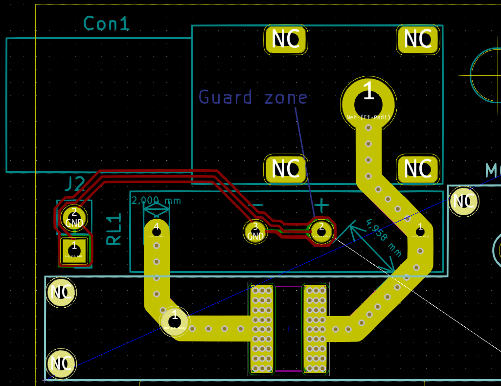
This is a 6-layer pcb. There is no ground plane off course. You can see the input HV connector that goes through the DC blocking HV cap and the HV reed relay. The yellow traces that you see, exist on 5 of the 6 layers. The vias were placed in order to further reduce impedance but since we are talking AC here, the signal path will be different compared to a DC signal. I do realize that vias add unwanted (parasitic) inductance. It all comes down to the BW, though. If we are talking 5MHz then i will be probably be fine. The probe that i am building, however, targets a 250MHz BW where things get more difficult. There is also a guard zone between the + of the reed relay coild and the high impedance input.
What do you think is better here? Single or multiple layers trace? Vias across the traces or not?
Do you know of any tools that do PCB simulation?
Regards
Manos Tsachalidis


