This thread has been locked.

If you have a related question, please click the "Ask a related question" button in the top right corner. The newly created question will be automatically linked to this question.

OPA847 oscillations with demo board

Other Parts Discussed in Thread: OPA847

Hi,


  I am a graduate student at the Indian Institute of Science. I am designing an amplifier using OPA847  for a gain of 1000 and noise <= 3 nV/sqrt(Hz). My final operating frequency is 1.5 MHz. I tried the demo board for SOT 23-6 packages. 

   I use a non inverting configuration with gain=51 (1+2500/50). There is a capacitor 0f 22 pF acroos the feedback resistor 2.5 KOhm. I am using two capacitor for power supply bypass (4.7 uF tantalum, 100 nF ceramic).

 The circuit oscillate around 25 MHz. Please help me sort out the problem.


  • Koushik,

    What is the purpose of the 22pF capacitor in the feedback? Are you trying to do some kind of equalization - high gain at low frequencies and no gain (0dB) at higher frequencies?

    If you are observing the oscillation on the scope, the apparent 25MHz frequency may be the beat frequency of several higher frequency oscillations. I believe the oscillation is really at higher frequencies, i.e. >100MHz. Try zooming in your time scale, from 10s of ns/div to 10s of ps/div - I expect that it may become harder to distinguish the oscillation frequency as you zoom in. Is that true?

    Given your circuit, oscillation is expected due to the large feedback capacitance. If you are trying to do some filtering, I would recommend placing the filter at the op amp output. When using a decompensated amplifier (non unity-gain stable) such as the OPA847 in the non-inverting configuration, placing the right values of capacitance across the feedback resistor can lead to oscillation, even if the DC gain is high.

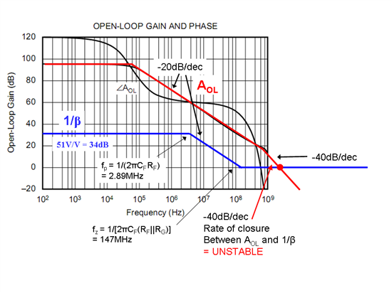
    See the closed loop gain plot (1/B) with the OPA847 open loop gain plot below. At low frequencies, the closed loop gain is 51V/V (34dB). You can see that the feedback capacitor adds a pole and zero to the closed loop gain and causes the closed loop gain to cross the open loop gain (AOL) at a rate of closure of -40dB/dec (rate of closure = slope of open loop gain - slope of closed loop gain = -40 - 0 = -40dB/dec). A -40dB/dec rate of closure corresponds to a phase shift of -180°, which, when added to the built-in -180° due to the op amp's negative feedback, results in a total phase shift in the amplifier loop of -360°:  positive feedback and ideal conditions for oscillations. For more information on op amp stability, click on this link to a TI-contributed article series on op amp stability:  http://www.en-genius.net/site/zones/acquisitionZONE/technical_notes/acqt_092407

    Again, I would suggest removing the feedback capacitor and instead implementing any filtering at the amplifier output.

    FYI - in my analysis above, I ignored the effect of the parasitic capacitance at the inverting pin of the OPA847, which will also modify the closed loop gain.

  • Hi Kristoffer,

         Many thanks for your help. The moment I removed the feedback capacitor, the oscillations vanish. I had used it to limit my bandwidth. As you suggested, I will use a filter with 5 MHz cutoff at the output of the opamp.

     As you suggested, I tried detecting for 100 MHz signal. But could not.  


    1)  I also get a large dc offset of around 800 mV. This will be a problem if I use one more stage of amplification (Gain=30). How do I minimize the dc offset? 

    I use a 50 ohms shunt resistance at the non inverting input. The inverting input is grounded via 50 ohms and thee feedback resistor is 2.5 Kohms.   


    2) Secondly if I use a filter (butterworth LC low pass filter) at the opamp output, there will be large reactive loading on the opamp output. Will adding 100 ohms at the output pin of the opamp help?


    Thanks

    Koushik

  • Koushik,

    With a gain of 51V/V, the 800mV offset implies about 16mV offset at the input, which far exceeds the offset I would expect from the input offset voltage and the input bias/offset currents combined. For example, the max input offset voltage over temperature is listed as +/-0.6mV. Assuming a worst case -42uA bias current flowing through the 50ohm resistance adds another ~2.1mV.

    Are you operating split supply (+/-5V) and is your signal bipolar, swinging about GND? Your input signal itself may have a DC offset.

    See the section called "DC Accuracy and Offset Control" starting on p.17 of the OPA847 datasheet. In particular, see the offset adjustment circuit suggested in Figure 15. The idea is that the op amp is being operated in a difference/summer configuration, and a DC voltage is applied to cancel out the unwanted offset at the signal input. Of course, the circuit will have to be modified for your gain and because you are using the op amp in a non-inverting configuration.

    Although the bias current is not the major cause of the offset, the bias current cancellation can be optimized. Is your input signal coming from a 50ohm source? For optimum input bias current cancellation, the effective impedance looking out of the non-inverting pin should be the same as the impedance looking out of the inverting pin of the OPA847. Due to the large feedback resistor (2.5kohm), the effective impedance looking out of the inverting pin is basically just the gain setting resistor of 50ohms. On the non-inverting side, the equivalent impedance is 25ohms:  the 50ohm source in parallel with the 50ohm shunt termination resistor. To match the effective 50ohms at the inverting pin, add a 25ohm series resistor between the shunt 50ohm resistance and the non-inverting pin itself.

    Regarding the LC filter, yes, you will definitely want to isolate the op amp output from a reactive LC load with a series resistor. You may only need a 10-30ohm resistor to remove any frequency response peaking. If you have a network analyzer, then you can easily test different resistor values to see what minimum value gives sufficient frequency response flatness. Alternatively, you can use an oscilloscope to observe the output with a square wave input to see what minimum resistor value gives you an acceptable pulse response with minimal ringing and overshoot.