This thread has been locked.

If you have a related question, please click the "Ask a related question" button in the top right corner. The newly created question will be automatically linked to this question.

INA230: The variation of Vbus input impedance

Part Number: INA230

Dear Technical Support Team,


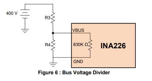
The datasheet shows that the input impedance of VBUS is 830kΩ(typ).

In my case is show about 890Ω with 500 samples.

I have some questions about it.


1. Is 830kΩ±15% related with the Vbus voltage ?

The example circuit(Figure 23) of datasheet shows that Vbus is supplied 12V. In my case, the Vbus is supplied 3.3V.

If you have the graph such as "X: Vbus voltage vs Y: input impedance", could you share it?

2. Is it possible to vary the input impedance depends on a lot number?

3. Could you provide internal circuit for VBUS?

4. If you have any reason of input impedance variation, could you share it?

According to following E2E, the input impedance variation is based on fabrication processes

and adjusted to keep Bus Voltage Gain Error on Datasheet. (10 ppm/C typical and 50ppm/C maximum)


https://e2e.ti.com/support/amplifiers/f/14/t/796587?tisearch=e2e-sitesearch&keymatch=ina230%20830


Best Regards,

ttd

  • Hi,

    1 the input impedance, 830kΩ±15% is independent of the Vbus voltage, whether 12V or 3.3V. There is no need for such a graph.

    2 It is impossible to know the exact resistance value based on lot number. You’d have to measure it.

    3 The internal circuit on this pin is a simple resistor divider which takes the MAX Vbus down to within the range of the ADC input. The total value of the divider is 830K.

    4 In a typical fab process, resistors match (ratio) well yet their absolute values are poor. In order to achieve an accurate absolute resistance, trim is required. Fortunately for Vbus pin, ratio matters and absolute value doesn’t at all, because Vbus is measured based on a ratio.

    Please let us know if you have further questions.

    Regards, Guang

  • Hi Guang,

    Thank you for your reply.

    >Fortunately for Vbus pin, ratio matters and absolute value doesn’t at all, because Vbus is measured based on a ratio.

    ⇒Does it mean following circuit of TIDU849 ?

       I think that if R4 is mush smaller than 830kΩ, the variation of 830kΩ is not large affect, right?

       http://www.ti.com/lit/ug/tidu849/tidu849.pdf   

    In my case, Vbus pin is connected between external 15kΩ(high accuracy) and internal 830k. These 15kΩ and 830kΩ are connected in series.

    Then ADC of INA230 shows approximately  3.25V, so I measure the ratio of series resistance that internal register is 890kΩ.

    The variation of  internal 830kΩ causes accuracy error in my system.

    So I will calibrate it through software. 

    Best Regards,

    ttd

  • Hi,

    You’re exactly right – if R4 is made much smaller than 830K, then the error effect of the Vbus pin input resistance is negligible in Figure 6.

    If you only have a 15K in series with Vbus pin, it will form a voltage divider with 830K. The effect is that measured bus voltage is a portion of what it actually is. You can certainly calibrate the measurement. Is there any reason in keeping the 15K? Why not just short it out.

    Regards, Guang

  • Hi Guang,

    Thank you for your reply.

    I understood about Figure 6.

    15kΩ resistance is thermistor.

    Best Regards,

    ttd

  • Hi ttd,

    Great, I think your issue is now resolved. But please confirm by clicking the “this resolved my issue” button. Thank you in advance.

    Regards, Guang