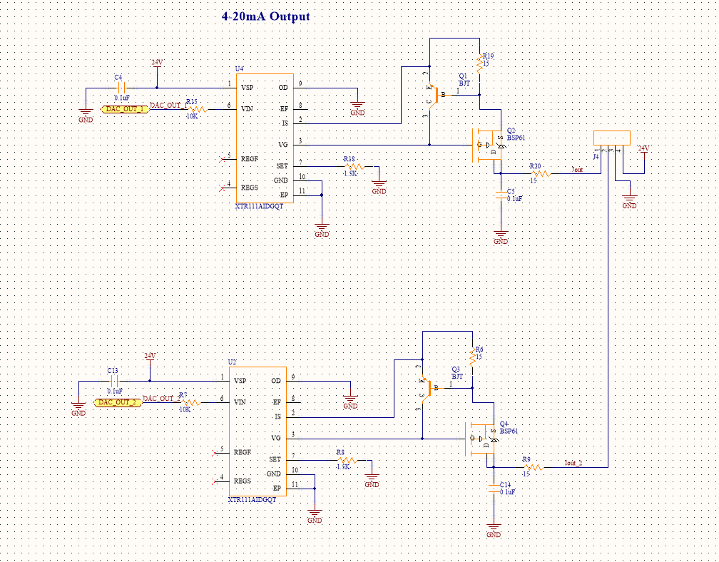
Part Number: XTR111
When i powered up my device the output is correct but after powered up the device mosfet start heating and continuously increases.
Attached schematic of the design,
MOSFET Used - BSP170
BJT Used - 863-SMMBT2907ALT3G
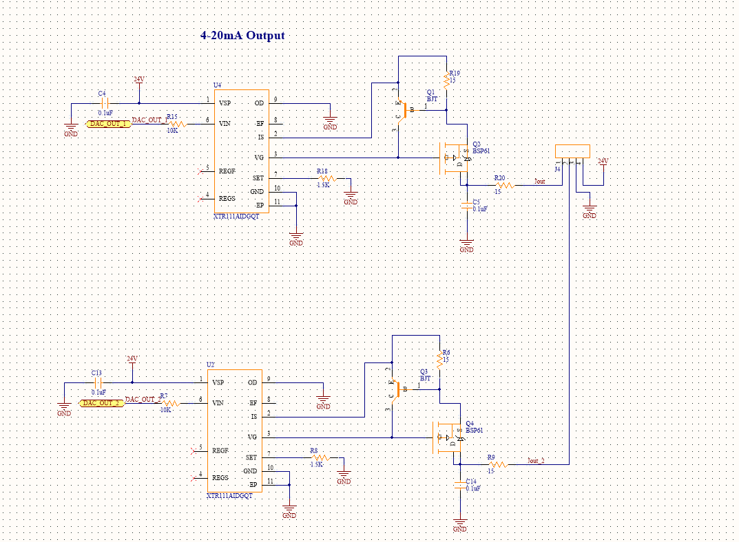
Part Number: XTR111
When i powered up my device the output is correct but after powered up the device mosfet start heating and continuously increases.
Attached schematic of the design,
MOSFET Used - BSP170
BJT Used - 863-SMMBT2907ALT3G