This thread has been locked.

If you have a related question, please click the "Ask a related question" button in the top right corner. The newly created question will be automatically linked to this question.

PGA280: Worst Case Analysis Help

Part Number: PGA280
Other Parts Discussed in Thread: PGA281

Team, 

I am helping out with some worst case analyses and am having trouble helping spec the max and min rated voltage on the pins as well as the current. can you help me with the below?
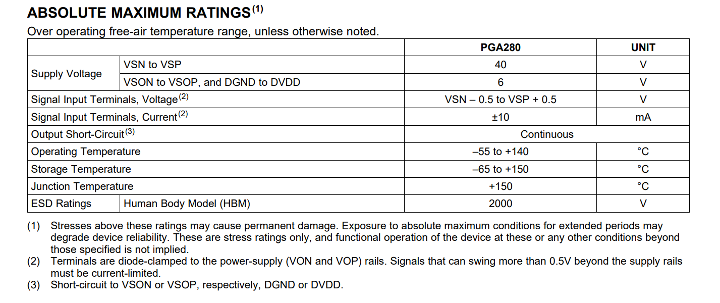
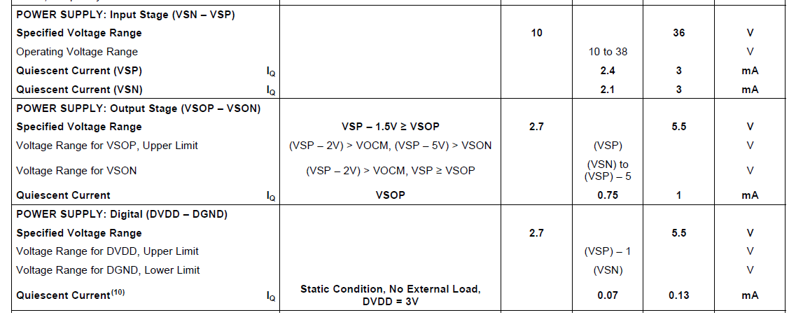
 

Description Part Number Package Pins Rated Pin Voltage (VMax) Rated Pin Voltage (VMin) Rated Pin Current (A)
IC OPAMP PGA 1 CIRCUIT 24TSSOP PGA280AIPW 24-TSSOP 24 - - -
VON: Inverting signal output PGA280AIPW 24-TSSOP 1      
VOP: Noninverting signal output PGA280AIPW 24-TSSOP 2      
VOCM: Input, output common-mode voltage PGA280AIPW 24-TSSOP 3      
VSOP: Positive supply for output PGA280AIPW 24-TSSOP 4      
VSON: Negative supply for output, AGND PGA280AIPW 24-TSSOP 5      
VSP: Positive high-voltage supply PGA280AIPW 24-TSSOP 6      
INP2: AUX input, noninverting PGA280AIPW 24-TSSOP 7      
INN2: AUX input, inverting PGA280AIPW 24-TSSOP 8      
INP1: Signal input, noninverting PGA280AIPW 24-TSSOP 9      
INN1: Signal input, inverting PGA280AIPW 24-TSSOP 10      
VSN: Negative high-voltage supply PGA280AIPW 24-TSSOP 11      
DGND: Digital ground PGA280AIPW 24-TSSOP 12      
DVDD: Digital supply PGA280AIPW 24-TSSOP 13      
SDO: SPI slave data output PGA280AIPW 24-TSSOP 14      
SDI: SPI slave data input PGA280AIPW 24-TSSOP 15 DVDD 0  
SCLK: SPI clock input PGA280AIPW 24-TSSOP 16 DVDD 0  
CS_N: SPI chip slect input; active low PGA280AIPW 24-TSSOP 17 DVDD 0  
GPIO6: GPIO 6, SYNC (in), OSC (out), ESC6_N PGA280AIPW 24-TSSOP 18 DVDD 0  
GPIO5: GPIO 5, BUFA (out), ECS5_N PGA280AIPW 24-TSSOP 19 DVDD 0  
GPIO4: GPIO 4, BUFT (in), ECS4_N PGA280AIPW 24-TSSOP 20 DVDD 0  
GPIO3: GPIO 3, EF (out), ECS3_N PGA280AIPW 24-TSSOP 21 DVDD 0  
GPIO2: GPIO 2, ECS2_N, MUX2 PGA280AIPW 24-TSSOP 22 DVDD 0  
GPIO1: GPIO 1, ECS1_N, MUX1 PGA280AIPW 24-TSSOP 23 DVDD 0  
GPIO0:GPIO 0, ECS0_N, MUX0 PGA280AIPW 24-TSSOP 24 DVDD 0  
  • HI Michael,

    Are you referring to the absolute maximum ratings, in other words, the voltages and currents the device can withstand without damage during a fault condition?If yes, please refer to the Absolute Maximum Ratings table on p. 2 of the datasheet. The below are the voltages/currents the device can withstand during a fault condition per the Absolute Maximum Ratings.  Please note these are not the same voltage range conditions specified for normal operation.

    The VSOP-VSON potential has to be less than 40V absolute maximum (Device is only specified for 36-V operation). 

    The INN and INP input terminals can withstand a min. voltage of VSN-0.5V and max voltage of VSP+0.5V during a fault condition. 

    The INN and INP input terminals can withstand a max. current of +/-10mA on a fault condition.

    VSON to VSOP, and DGND to DVDD supply max voltage is 6V during a fault condition, (Also DGND should not be at a potential below VSON, per electrical characteristic table on p5.)

    All the digital inputs (CS, SCLK, SDI, GPIOs)  can not be at a potential below DGND or a potential above DVDD, and can withstand a max current of +/-10mA)

    The analog output should not exceed VSON or VSOP supply voltage or the specified short circuit current.

    The Digital Output voltage should not be at a potential below DGND or a potential above the DVDD supply voltage or should not exceed the specified source/sink circuit current. 

    Thank you and Regards,

    Luis

  • Luis, Thank you for your help!

    I am refereing the the maximum that each pin can see during normal operation (i.e. recommended operating conditions that will allow the device to operate within the spec) 

    So not the abs max unfortunately. 

  • Hi Michael,

    Thank you for the clarification. 

    Please refer to the Electrical Characteristics Table on pages 3-5 where the voltage/current ranges for the supplies, input and output pins is specified. 

    For example, the voltage range of the VSP, VSN high voltage supplies, the VSOP,VSON output stage voltage supplies, and the Digital power supplies (DVDD/DGND) voltage and current ranges are listed below: 

    The VSP-VSN input stage supply voltage difference should be in the range of 10V to 36V; max quiescent current is 3mA. 

    The VSON/VSOP output Stage voltage difference must be from 2.7V to 5.5V; max quiescent current is 1mA.  VSP must exceed VSOP by at least 1.5V.  Also, VSP must exceed VOCM pin by at least 2V and the VSP input supply must exceed the VSON output negative supply by at least 5V.  The VSON negative output stage supply must be greater or equal to the input negative supply voltage VSN.

    The digital supply DVDD-DGND potential is spec in the range of 2.7V to 5.5V, with 0.13ma max quiescent current. DVDD must not exceed (VSP) - 1V and DGND must be at a voltage equal or grater than VSN.  

    In similar fashion, the analog inputs, PGA281 output and all digital inputs/output voltage ranges and drive capability is specified in detail on the table. However, please let me know if you require a clarification. 

    Thank you and Regards,

    Luis