This thread has been locked.

If you have a related question, please click the "Ask a related question" button in the top right corner. The newly created question will be automatically linked to this question.

Fault pin always active and a lot of current consumption

Part Number: TPA3221
Other Parts Discussed in Thread: LM340, LM393, MSP430F5529

Hello,

I'm developing a portable audio speaker and I want to use the TPA3221,but at this time, I can't make it work.

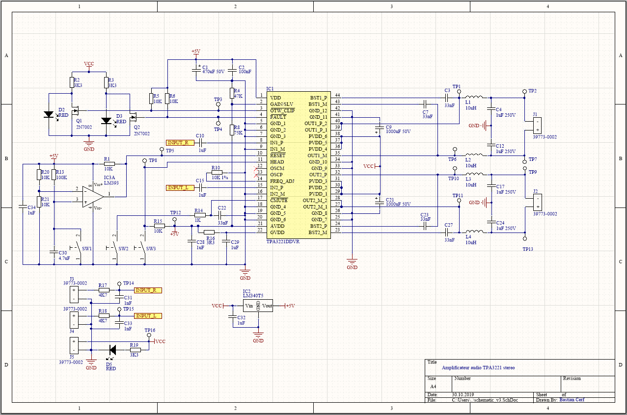
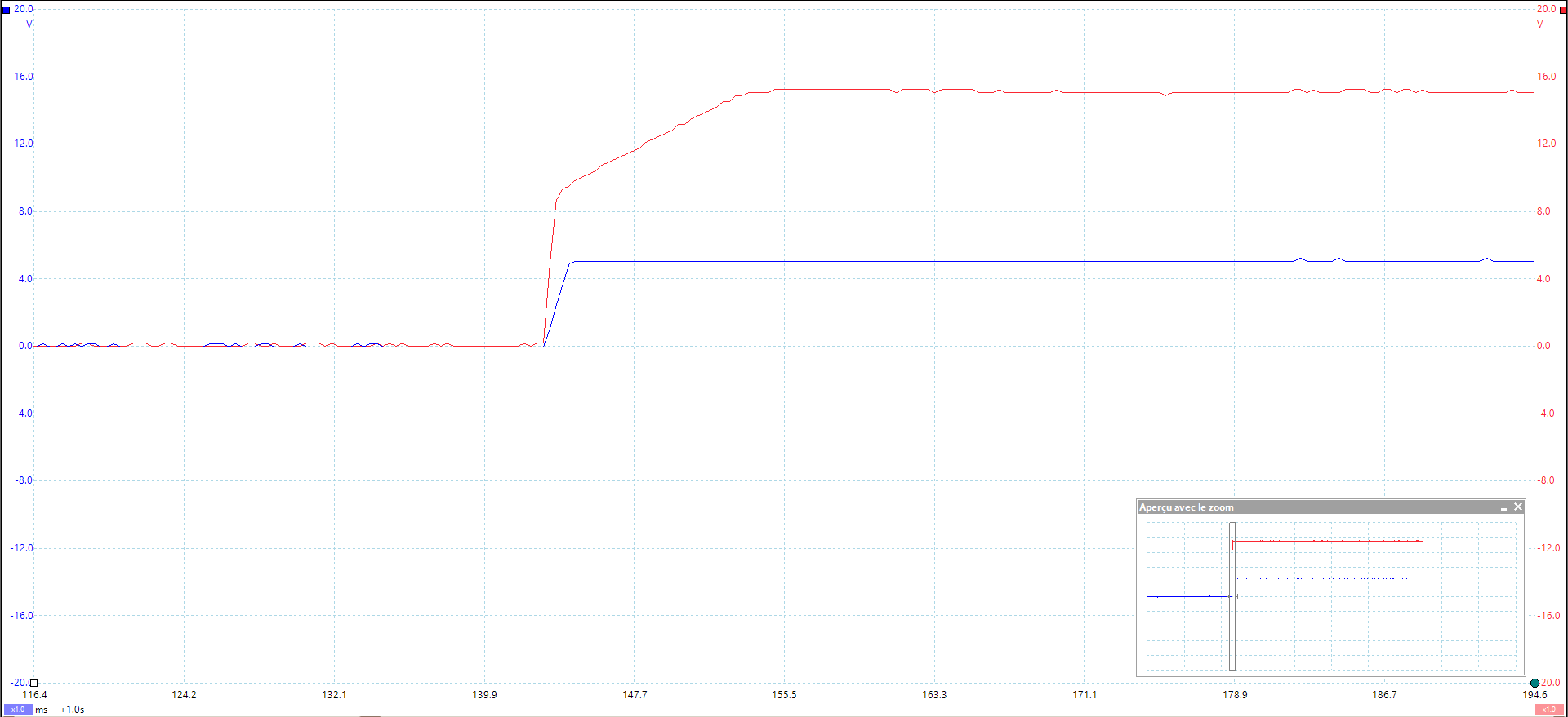
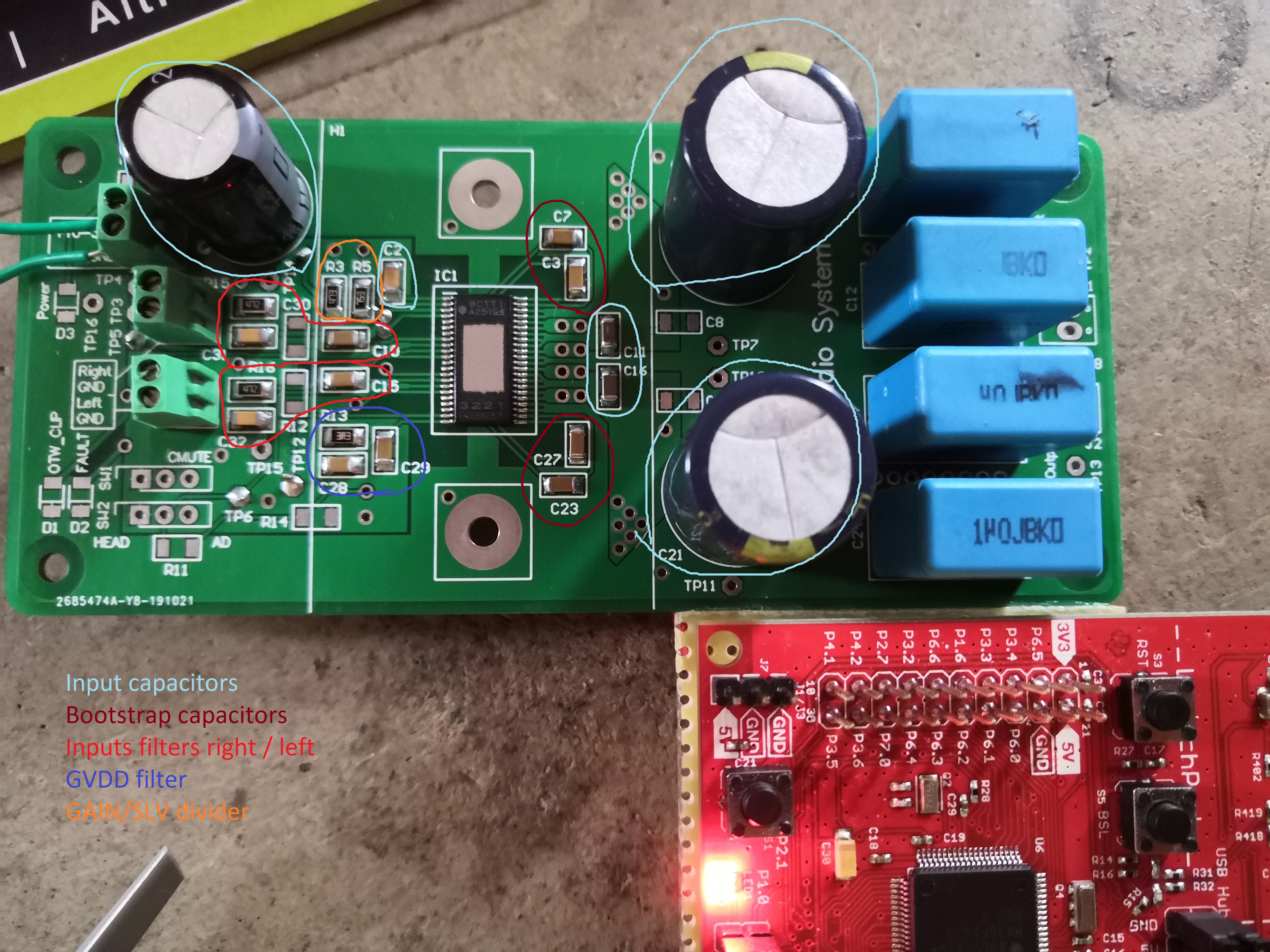
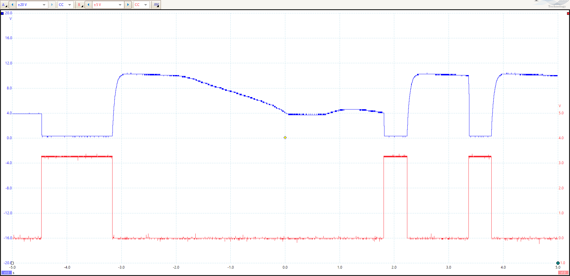
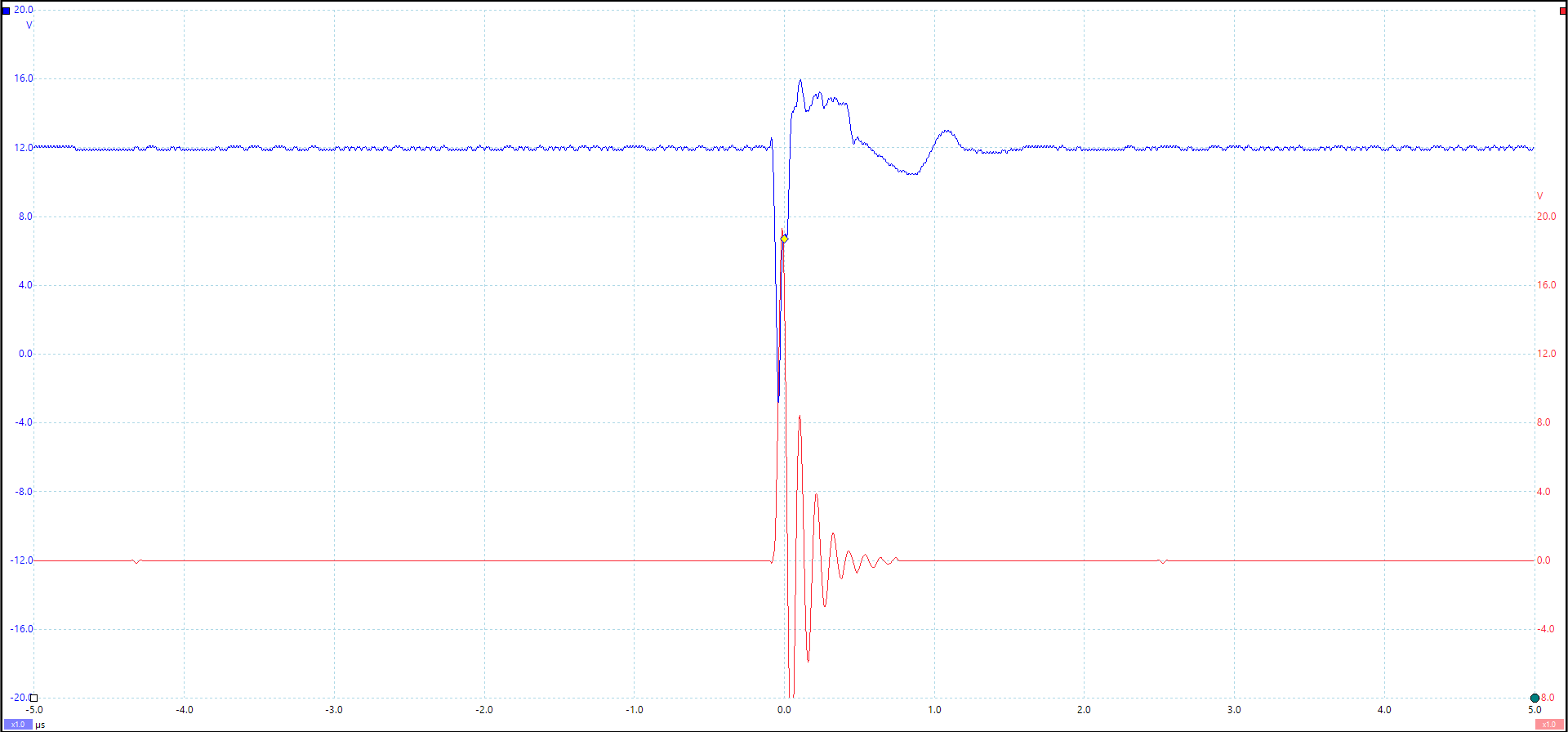
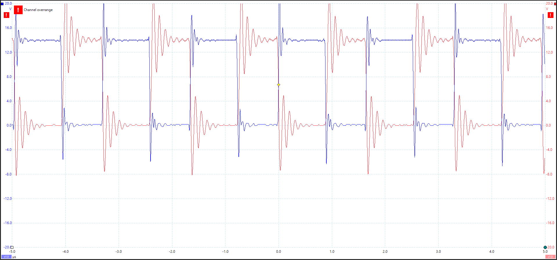
I designed a test board and this is what I noticed in my tests :

- Nothing on the outputs, little crackling when a speaker is connected

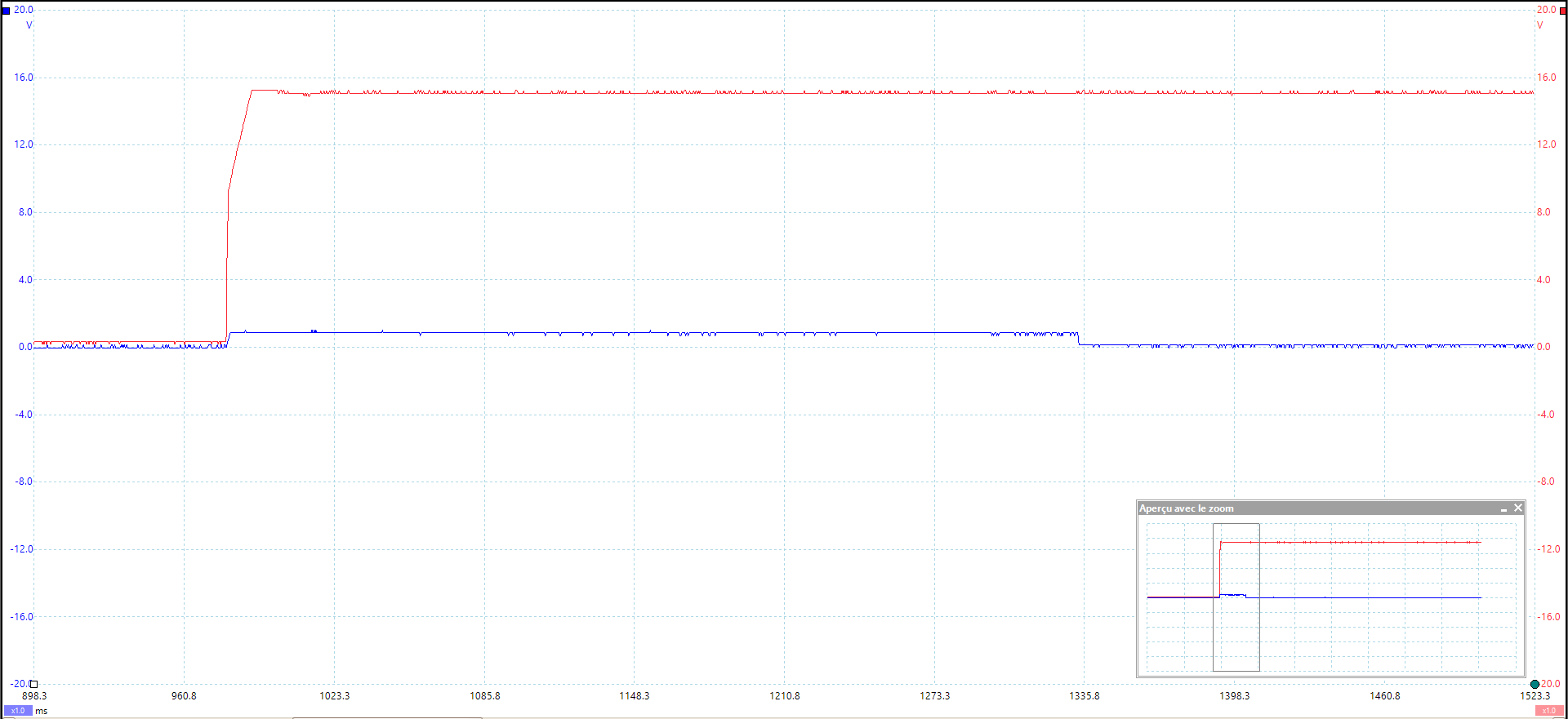
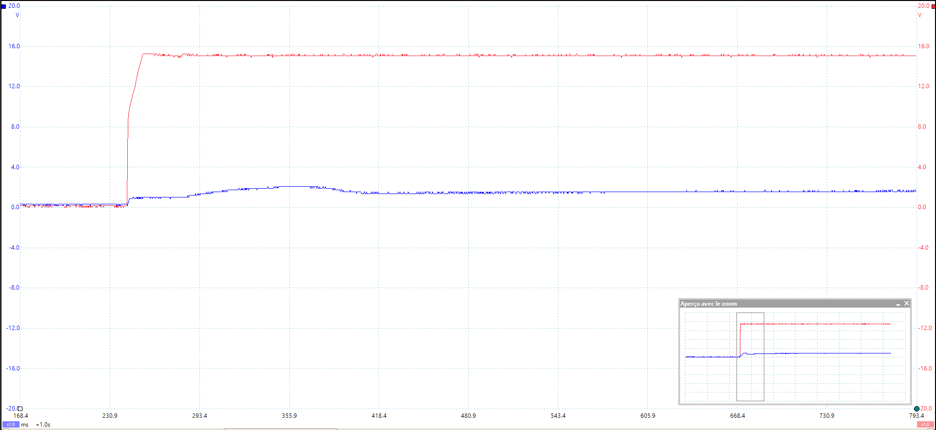
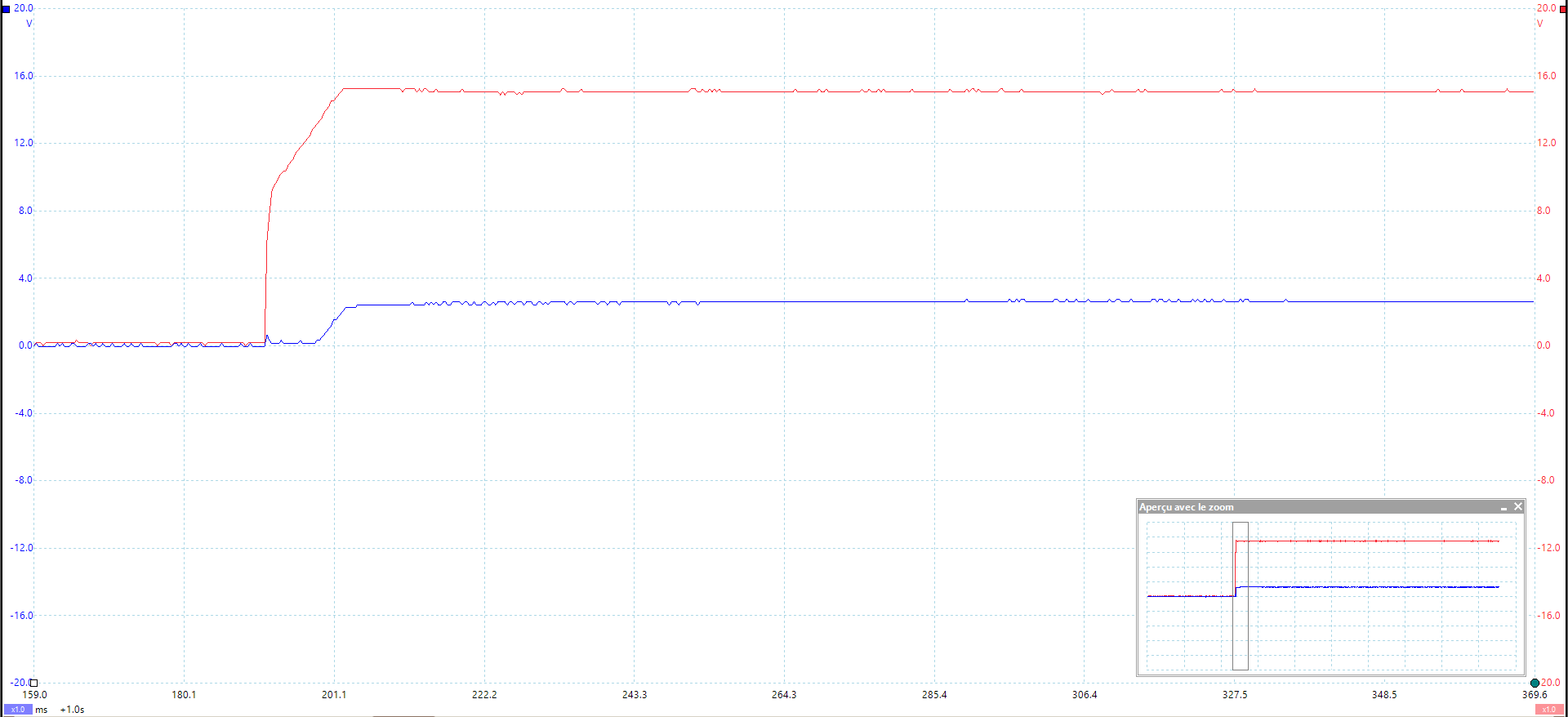
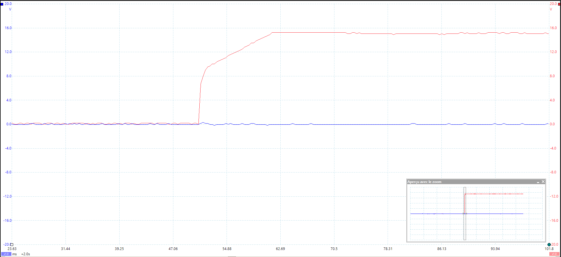
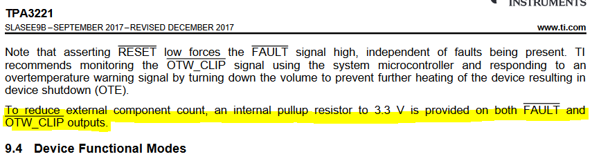
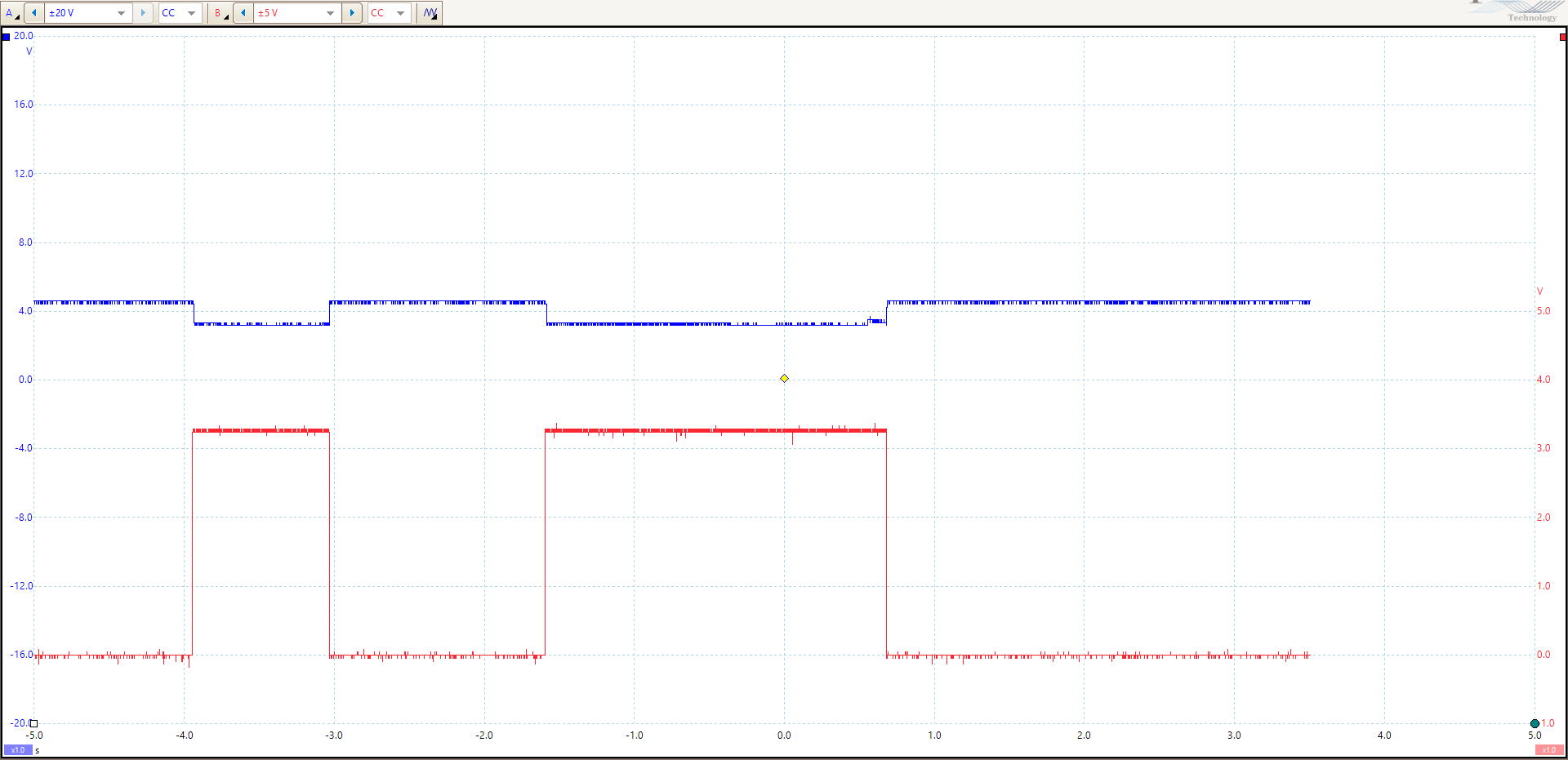
- When the reset is low, otw_clip and fault are off (5V by pull-up)

- When I put reset to high state, fault led goes on

- Current consumption never above 100mA

- The 5V internal LDO stays at around 4V with peaks to 4.5V but it never reaches 5V.

I tried to use an external supply (basic LM340T5) to power the VDD, AVDD and GVDD instead of the internal LDO, but nothing changed.

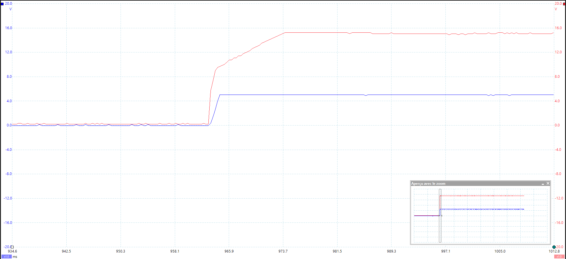
So, I decided to replace the TPA3221 IC. Here is the result :

- Nothing on outputs

- Fault LED always on, even if the reset is low

- Current consumption around 250mA (strange thing... )

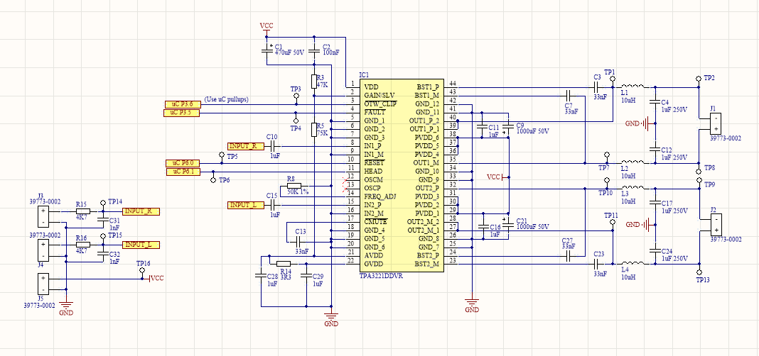
This is my current schematic :

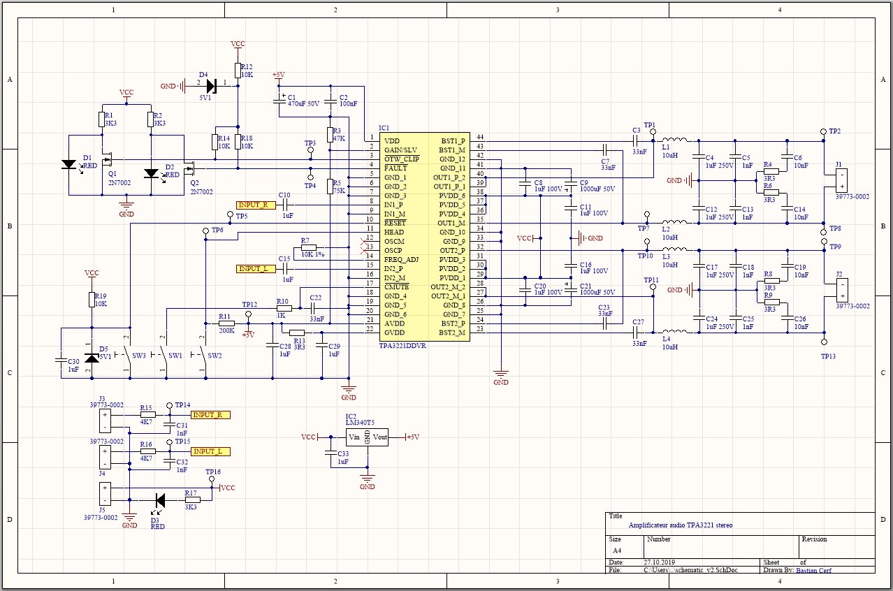
Do you think my board has damaged the TPA3221 ?

Inductors are SRN1060-100M from Bourns.

C9, C21, C4, C12, C17 and C24 are the same as on the EVM board (PHE426HB7100JR06 and EEU-FC1H102).

I can send you the schematic and the PCB in altium format if you prefer.

I have an other question about the filters behind the TPA3221. What are the filters formed by C5, C6, C13, C14, R4 and R6 for ? I only see them in the datasheet but nobody uses it.

Thank you in advance for you help and sorry for my english :-)

Best regards,

Bastian Cerf

  • Hello Bastian,

    Can you confirm if your startup sequence is the same as the one outlined in section 9.4.1 in the TPA3221 datasheet by seeing if PVDD, GVDD, AVDD, and VDD are stable before you change reset from low to high.

    Also to answer your question about C5, C6, C13, C14, R4 and R6. Those make up a zobel network, which is primarily speaker dependent and compensates for the speaker's inductance affecting its impedance in high frequencies. In our EVM we have it as optional so the designer can determine whether it's a consideration in their design or not.

    Best Regards,

    Luis

  • Thank you very much for your answer, I didn't know the zobel network before.

    I made a new board and I have changed a little the schematic. Now, I only use the 5V supply from the LM340 instead of the two zener diodes for the pull-up and RESET. I have removed the zobel network (to have my board as simple as possible) and I have used a basic RC with a LM393 to generate the RESET signal.

    This is the schematic :

    The board consumes only 20-30mA (with a new TPA3221), but I have the same problem than before. The fault led is always on and sometimes the otw_clip's led too.

    I have done the startup measures. In each picture there is the PVDD voltage in red and the other signal in blue.

    VDD :

    GVDD :

    RESET/ :

    AVDD :

    Same as VDD.

    FAULT/ :

    It's like if the fault pin tries to go high but can't ...

    IN1_P :

    OUT1_P (TP1 on my schematic)  :

    There is no speaker on the outputs.

    OUT1_M :

    Same as OUT1_P.

    CMUTE/ :

    It never charge.

    An other strange thing (or not ?) I have noticed is that the voltage on GAIN/SLV must be around 1.9V (47K and 75K), but I measure 4.8V, I don't know if it's normal in the TPA3221 operations.

    I have seen this in the datasheet :

    Maybe the device initializes in slave mode ? OSC_IO are open so it can explain why it stucks at fault.

    I can give you more accurate measures with more than 2 channels together if needed.

    But it's very strange because the fault pin doesn't go high when RESET is low, like it is said in the datasheet :

    Thank you for your help !

    Best regards,

    Bastian Cerf

  • Hello Bastian,

    The 4.8V does not seem like the correct value and if that is what the GAIN/SLV is seeing your device might be in slave mode and you would encounter this error where you are stuck at fault. Can you do a sanity check and measure the resistors you are using R8/R4, or try using different resistors values for a different gain setting to see if you are seeing the same behavior on that pin.

    Best Regards,

    Luis

  • Hello Luis,

    I tried to change the voltage divider but the TPA3221 puts ~4.8V on the pin, even when there is no resistor. The board is clean.

    It's strange because I measure ~70 ohm between the pin and VDD. It's like a 70 ohm resistor is internally connected between VDD and GAIN/SLV.

    Is there an explication or the IC is damaged ?

    Best regards,

    Bastian

  • Hello Bastian,

    If you are measuring 70 ohms, that is indicative of a short on your board between GAIN/SLV and VDD. You might want to do more continuity tests on your board, check your layout, and check the soldering on your board.

    Best Regards,

    Luis

  • Hello Luis,

    Sorry for the long time to answer. I have done many tests and it seems that my new solder flux leaves conductive residues on my board. It explains why I had some random behaviors. So I have built a new prototype board and I clean it with isopropanol. The voltage on GAIN/SLV is correct (~1.93V). For this new prototype, I'm using my new MSP430 launchpad board (very cool tool !).

    So, the problem is simple. The fault pin always goes low when the reset pin is pulled high. I have noticed that the CMUTE capacitor never charges and I think it's for this reason I have nothing on the outputs. How can I be sure that the outputs are in high-Z state ?

    This is a picture of the prototype, maybe it could help.

    This prototype corresponds to this schematic :

    I have tried to power the TPA3221 with an external LM340 and the result is the same as when I use the internal LDO.

    I don't know the reason why CMUTE doesn't charge, so I don't know which measures can be useful to find the problem ..

    Thank you very much in advance !

    Best regards,

    Bastian

  • Hello Bastian,

    What is your PVDD voltage, and what current is your power supply rated for. Also I noticed in your board your test points on the output stage are inside your output traces. This will cause issues.

    Best Regards,

    Luis

  • Hello Luis,

    I use my laboratory power supply for my tests. I use a voltage of 24V, and I can have more than 3A on output. I've tried with a lipo battery of 22.2V / 25C too, but the result is the same. The current is 45mA when RESET is high and 25mA when it is low.

    Which test points are you talking about ? I did the best I could to follow the layout example provided in the datasheet at 12.2.1. Can you have a look to the gerber files ? I have done 3 prototypes that all have the same problem and the only common point is the PCB that I've used with the TPA3221. Do you see a problem with the routing of the output stage ?

    Gerber files : test_board.zip

    Thank you very much in advance !

    Best regards,

    Bastian

  • Hello Bastian,

    After looking at your gerbers it doesn't seem like a point of concern, based on just the picture it was hard to tell. I will need time to investigate your problem further. Thank you for your patience.

    Best regards,

    Luis

  • Hello Luis,

    No problem ! Thank you very much for your help. If I notice something new I'll let you know.

    Does the TPA3221 have an internal 3.3V LDO ? Otherwise I don't understand how this is possible :

    If it has a pullup, what's its value ?

    It's very strange because I measure 5V on OTW_CLIP (no pullup or pulldown) when RESET is high.

    Thank you very much again.

    Best regards,

    Bastian

  • Hello Bastian,

    See OTW/SHUTDOWN section in the Electrical Characteristics table in the datasheet and section 9.3 in the datasheet for details about pull-up value and internal LDO. There is only a 5V internal LDO, not a 3.3V this is an error. The value is 5V for the pull-up you are correct, the datasheet is being updated to correct this issue where it says it is a 3.3V rather than 5V. 

    Best Regards,

    Luis

  • Hello Luis,

    Fortunately, the pull-up of the MSP430F5529 was activated and has made a voltage divider with the 5V pull-up of the TPA3221. So I notice no damage.

    I have done some measures on the outputs and it's very strange. When reset is low, I measure ~4V between all outputs and GND. If I do a short with GND, the voltage always returns to ~4V. This is what happens when reset is high (reset in red, output_x in blue) :

    OUT1_P :


    OUT1_M, OUT2_P, OUT2_M :

    Only OUT1_P has a different behavior.

    I hope it can help.

    Best regards,

    Bastian

  • Hi Bastian,

    If Reset is low, all the outputs is set to Hi-Z. 4V measured on the outputs indicates it is not working well.

    In normal operation, OUTx_P/M pin waveform should be square wave. In the pictures, looks like non of the output is in square wave. 

    Could you check the soldering of GVDD and OUTx pins? Measure the forward voltage drop of ESD diode on each pin would be a good method. The normal VF should be 0.4~0.7V.

    Thanks!

    Regards,

    Hao

  • Hello Hao,

    When I was measuring the VF on each diode, I noticed that a BST capacitor was defective (It's the first time ever I see a defective ceramic capacitor, maybe I did a wrong manipulation...). So I have changed it, and the behavior of the board has completely changed !

    The VF of ESD diodes seems correct (0.3V for VDD, AVDD, GVDD and 0.5V/0.7V for the others).

    This is the new behavior of the board : On power on, everything is normal (OTW_CLIP and FAULT high, supply current ~35mA). Then RESET goes high  and OTW_CLIP goes low but the IC doesn't heat (supply current of ~100mA). The PWM try to start (see fig.1). The CMUTE capacitor is correctly charged. Then I toggle CMUTE, OTW_CLIP goes high and the PWM starts (fig.2).

    When OTW_CLIP is low the offset voltage on outputs is ~12V. When the pwm has started, the offset is ~1.3V and I can have some music on outputs with a lot of distortion in bass frequencies.

    Fig. 1 (blue : OUT1_P, red : OUT1_M, scale : 1us/div) :

    Fig. 2 (blue : OUT1_P, red : OUT1_M, scale : 1us/div) :

    If needed, I can have more accurate measures with an other scope.

    Do you have an idea why the pwm never starts on first time ? What can cause the offset voltage ? Maybe the BST capacitors have to be closer to the TPA3221 ?

    I hope that my explanations are clear, I do my best in english !

    Thank you very much for your help, this forum is just awesome.

    Best regards,

    Bastian

  • Hello Bastian,

    Can you try adding a 1uF cap to ground on the IN2_M and IN1_M, rather than directly shorting to ground.

    Best Regards,

    Luis

  • Hello Luis,

    You are a genius, it's working perfectly !! The music quality is pretty good. Now I can start designing the beta board :-)

    I don't know why I didn't use these capacitors before ...

    Thank you very much !!

    Best regards,

    Bastian