Because of the holidays, TI E2E™ design support forum responses will be delayed from Dec. 25 through Jan. 2. Thank you for your patience.

This thread has been locked.

If you have a related question, please click the "Ask a related question" button in the top right corner. The newly created question will be automatically linked to this question.

PGA308: Operating supply current

Part Number: PGA308

Hi team,

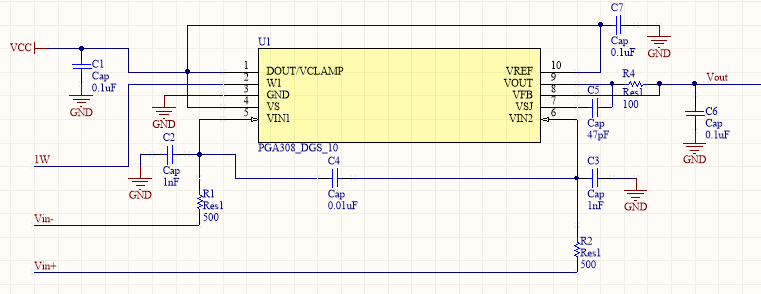
The circuit

designed by the customer according to the EVM board is shown in the figure below. The pin4 pin (vs pin) of PGA308 chip supplies 5V power. Connect the ammeter in series and test the working current of the chip. It is found that about 50mA, the chip can work normally. In datasheet, there is no parameter of working current, only the parameter of quiescent current IQ is 1.3mA. Is the working current of the chip 50mA normal?

Best Regards,
Amy Luo

  • HI Amy,

    The PGA308 power supply consumption is essentially the quiescent current, plus any load current at the output.  This is an instrumentation amplifier, therefore is relatively low power, with a quiescent current in the range of 1.3mA, and the maximum output current it can source/sink is around 10mA.

    The 50mA current consumption is abnormal, and the output has no load.  The expected current consumption of the circuit above is about 1.3mA.  The schematic above does not show anything obvious issue.  Is your VCC supply +5V?  Any chance the device has been exposed to ESD or an over-voltage condition?  Is the problem occurring on one PCB board or several PCB boards?

    If this issue is only occurring on one device, you may consider testing a fresh unit,  If this issue is occurring on several devices, kindly share the PCB board layout and the voltage supply conditions.

    Thank you,

    Kind Regards,

    Luis

  • HI Amy,

    I see the Customer voltage supply is +5V, as you have already stated on the original post... 

    If the Customer issue is only occurring on one device, please consider asking the customer to test a fresh unit, the unit may be damaged due to over voltage or ESD. 

    If this issue is occurring on several devices, kindly ask the customer to share the PCB board layout

    Kind Regards,

    Luis

  • Hi Luis,

    Thank you for your reply.

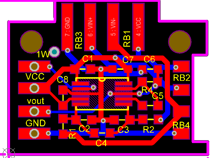
    Recently, the customer has tested several PCB boards and found that the working current is generally about 40-50mA. The following is the designed PCB layout:

    RB1, RB2, RB3 and RB4 in the figure correspond to 8 leads of 4 external strain gauges. The 4 external strain gauges on PCB have formed the Wheatstone bridge. The working current of the chip obtained by the test has reduced the working current of the Wheatstone bridge.

    Best Regards,
    Amy Luo

  • Hi Amy,

    1) Can you show the complete system circuit diagram or schematic when they connect the external Wheatstone bridge sensor, wheatstone excitation, power supply connections, and MCU or controller connections and MCU supply connections:

     - Include the PGA308 voltage supply circuit, sensor excitation voltage supply and MCU or controller supply connections and all ground connections. 

    -  Include the Wheatstone sensor connections and Wheatstone excitation voltage supply connections.

    -  Is the Wheatstone sensor excitation powered with the same 5-V supply or separate supply?  Is the Wheatstone excitation voltage referred to the same GND potential?  Please show a complete block diagram showing all the external wheatstone connections. 

    2) If separate supplies, Is the PGA308 supply powered prior powering up the Wheatstone excitation voltage?  Please note the VIN1, VIN2, 1W input pin voltages of the PGA308 must never exceed the PGA308 rail supplies during power-up or power-down or the PGA308 will be damage.  Please review the PGA308 Absolute Maximum Ratings of page 2 of the PGA308 datasheet.

    Thank you and Regards,

    Luis   

  • HI Amy,

    I have not heard from you, if the issue continues please post the information requested above.

      Thank you and Regards,

    Luis