This thread has been locked.

If you have a related question, please click the "Ask a related question" button in the top right corner. The newly created question will be automatically linked to this question.

ACF2101: ACF2101BU

Part Number: ACF2101
Other Parts Discussed in Thread: IVC102

Dear Support,

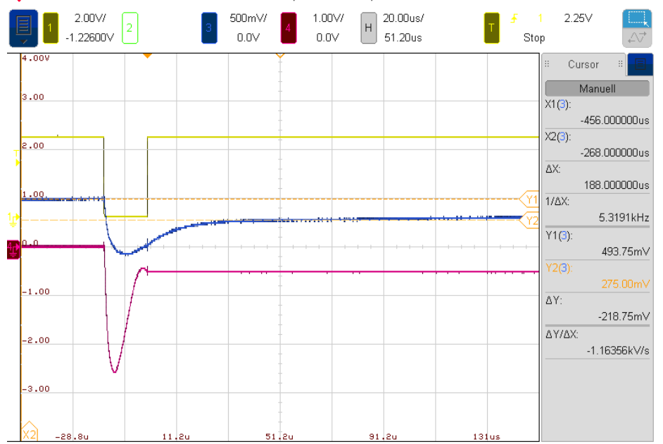
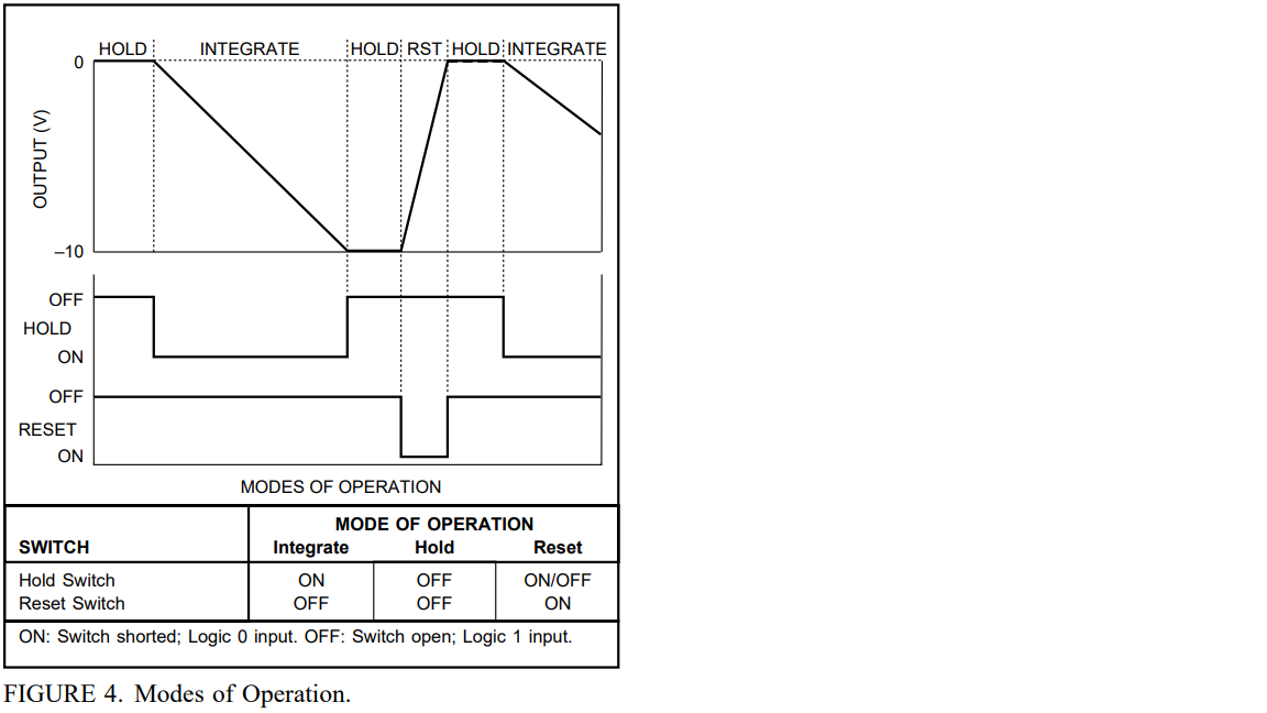
I am trying to configure the ACF2101 with current input. The power supply of the integrator is -15V, respectively +5V. I have applied a DC current of 0.1uA at the input from a current supply. I use the internal integration capacitor of 100pF and integrate for 16.7us. After the integration phase follows a hold phase and then a short reset phase (see attached timing diagramm). The phases are then repeated. The second integrator is never integrating (Hold is always on HI).

According to the formula in the datasheet I should get a voltage of 16.7mV at the end of the integration phase. However the output goes much higher (approximately 0.5V) and the integration curve looks weird (see attached oscilloscope screenshot).

I continuosly measured the voltage at the integrator’s input and this rises up to 0.5V, which is not desired – as I understood from the datasheet.

Color code of the signals on the screenshot:

Yellow: Hold signal

Purple: Output voltage, Integrator A

Blue: Input voltage (Sw In A)                                                                                                                                                                                      

Is any other circuitry necessary in order to get the output as expected?

Thank you for your help in advance.


  • Hi ,

    Your schematic seems to be ok. However, I think that you do not have the correct timing sequences shown in figure 9 of the datasheet. Also see Modes of Operation in Figure 4 of the datasheet. Make sure that you have the required reset time to discharge the 100pF, which it requires 5usec minimum, see p.6 of the datasheet.  

    Channel Select, Reset and Integrator output sequences have to be inside of Hold period, then the 100pF capacitor starts to integrate for 16.7usec (in your case) on the falling edge of fs clock frequency. I believe that the output voltage should be in saw tooth pattern (operated in the linear part of the capacitor charging curve). 

    Please try it again and let us know. 

    Best,

    Raymond

  • Hello Raymond,

    thank you for your reply.

    I do not use the Select channel at all. And as I see the Reset and Hold signals correspond to the timing diagramm on Fig.9. My Reset Signal was already longer than 5usec, but I made it even longer now. Please check my attached oscilloscope screenshot. Input current is 0.4uA now, Integration period is still 16.7usec and I use the internal capacitor of 100pF. My output voltage shold be -66.8mV. But I get -6.7V. 

    Any idea what could be wrong in my configuration?

    yellow: Hold

    green: Reset

    purple: Integrator output

    blue: Integrator input, SW IN  

    Thanks.


  • Hi ,

    ACF2101's ramp voltage at the output is a function of frequency of fs and 100pf integration capacitor in this case. The output voltage gain is described on p.11 of the datasheet, also see below. 

    During Reset, the output voltage should return to 0, see figure 4, which the 100pF cap is discharged. There should be two Hold period before and after Rest pulse. I do not see that from your capture plot. The integrator output should start with 0V and ramp downward (more negative) during integration (in saw tooth pattern).

    I think that your fs frequency is the issue. At the falling edge of fs frequency, it needs to stay low beyond Hold pulse, see Figure 9. It looks like the fs signal (ch4, purple?) goes high when reset is occurred. Also, the Ch3 (blue?), integrator output does not look right. On the rising edge of the Reset rising edge, the  integrator's output should return to 0V, see Figure 4 and 9. 

    Please follow Figure 4 modes of operation:

    During integration, Hold Switch is On (logic 0), Reset is Off (logic 1)

    During Hold states, both Hold and Reset switch are off (logic 1)

    During Reset period, Reset is On (logic 0) and Hold switch will On then Off. 

    I think that you are getting closer. Please let us know. 

    Best,

    Raymond

  • Hi Raymond,

    the problem is, I do not have any fs signal. In the datasheet the fs signal is a digital current input. But in my configuration I have a DC current input. This is why I thought, that I can determine the Integrator output through the formula from page 10.

    You wrote that my fs signal goes high, when reset occures. But the purple signal is the Integrator output, not the fs. Please see my legend to the screenshot signals at the end of my last reply.

    The output returns to 0 if reset occurs (see screenshot), as expected. And there are two Hold periods before and after my reset (see screenshot).

    Best regards,

    I Sandor


  • Hi I Sandor,

    Initially, I thought that integrator output (purple graph) may be mislabeled, that is why I placed a question mark on the reply. 

    The purple plot did show the integrate downward edge at Hold Switch=On and Reset=Off. For Input current is 0.4uA, Integration period is still 16.7usec and I use the internal capacitor of 100pF. My output voltage should be -66.8mV, which is based on Cdv/dt=i. However, the output voltage of ACF2101 is calculated based on the equation of Vout=Isensor * Rprogram. Rprogram is controlled by the fs frequency, see p.11-12 of the datasheet. 

    The timing generator is shown in Figure 11. If fs=10kHz, the Rprogram is equivalent to 1MOhm. Rprogram is equivalent to gain of the circuit. If you have fs=10kHz and Rprogram=1MOhm, the output is expected to be 0.4uA*1MOhm=0.4V. Based on your scope timing, you equivalent fs switch signal is approx. 1kHz, or Rprogram>10MOhm. That is why you see higher voltage than you expected. If you have fs=1kHz, then 0.4uA DC current will produced -4V output at.

    To back calculate your output at -6.7V, the equivalent fs is calculated to be approx. 597 Hz or 1.675 msec, which is not close to what the scope shot indicated. The scope shot indicated that your fs is approx. 800usec or 1.25kHz.  if you are integrating 16.7usec, your fs clock should be approx. at 59.9kHz, which I do not see from the scope shot. You have to select one of fs switch frequency from the table on to of p.12. Rprogram values are not linear in Rprogram vs. fs. 

    Rprogram=1/(fs*100pF) is based on Cdv/dt=i. Delta(V)=(i/C)*Delta(t), where Delta(t)=1/fs. This will give you Delta(V)=i/(fs*100pF), where Rprogram=1/(fs*100pF). So the circuit gain factor is determined by 1/fs for 100pF. Also, fs timing also determines how fast integrator output is latched out.  Hold, Reset and Select (you are not using) are very small portion of fs switching frequency. 

    DC input current is fine, but you will need fs is used to generate Reset and Select signals in Figure 11. You do not have to use the Figure 11 Hardware Timing generator. You can generate the Hold, Reset, Select timing signals from MCU. 

    Best,

    Raymond

  • Hello Raymond,

    now I think I understood, what do you mean regarding fs.

    I reconfigured the Reset and Hold signals, so that I have fs=1kHz. With an input current of 0.4uA I get now 4V. The following screenshot shows this (the legend of the signals is unchanged).

    However I would like to have a larger Hold period than that on the screenshot. This is why I modified the Duty cycle of the Hold signal, without changing fs of 1kHz. Up to a hold duration of approximately 250us the integrator still delivers 4V on ist output, as expected (see screenshot below). 


    Unfortunately for hold durations larger than ca. 250us the output deviates from the expected value and it rises to 4.55V (see screenshot below)

    What is the explanation for this? Thanks in advance.

    Best regards,

    I Sandor 

  • Hi I Sandor, 

    It is great that you got it working. 

    Regarding to "Unfortunately for hold durations larger than ca. 250us the output deviates from the expected value and it rises to 4.55V"

    Do you want to integrate the input current whatever your application is called out? If it is so, there is another mode which is described on p. 12, above Figure 10. However, you have to use Select switch (which is not used current). 

    Please let me know if this will work for your application.

    Best,

    Raymond

  • Hi Raymond,

    I need to use the Hold switch, because I must gain some extra time for the output acquisition to be terminated. So unfortunately this option does not work for me.

    I tried to increase the integrating capacitor by connecting an external 100pF to the integrator. I was curious if this influences the max duration of the hold signal (that of the ca. 250us I mentioned before), but it did not.

    I understand, that by increasing the hold duration, but keeping fs the same, the actual Integration time (where hold is LOW, reset is HIGH) gets smaller. But this should end after my expectation in a smaller value at the output of the Integrator. But I actually get a higher output.

    I still do not understand what this hold duration limitation is caused by.

    Best regards,

    I Sandor     

  • Hi I Sandor,

    For continuous current integration, hold should be small percentage of integration timing. In Figure 10, Cin is charging while Hold switch Open. When Hold switch is closed, the charge in Cin will transfer the charge to integrating capacitor. 

    You have a constant 0.4uA current source, when Hold switch is Open (250usec or longer), the IC is not integrating the current, that is why I am suggesting the alternative. 

    If you have an extra pin at your MCU, I will suggest to add Select signal to ACF2101. You may be able to integrate the current at lower fs frequency with 100pF. 

    In Rprogram=1/(fs*100pF) equation:

    fs at 1kHz, Rprogram=10MOhm or 1 msec period. 

    fs at 500Hz, Rprogram=20MOhm or 2 msec period

    fs at 300Hz, Rprogram=33.3MOhm or 3.33msec period (this may be the lowest frequency you can go, unless you change the negative voltage rail, lowest negative voltage is -18V on this part). 

    Please try the combination of Select, Hold and Reset in combination. From Figure 9, set Hold=closed, Select=Open, Reset=Off, when you want to end integration. With Hold=closed, Select=Closed, Reset=Open, when you want to start the next integration. 

    Try this combination, please let me know. 

    Best,

    Raymond

  • Hi Raymond,

    I have tried what you suggested and I get the following graph (green is Reset, yellow is Select, blue is Integrator output).

    Hold is completely off and Reset and Select are changing with the opposite sign. The frequency is 1kHz and the input current at SW_IN is 0.3uA. With this configuration I get 1.5V output. This is half of that what I expect. Modifying the current I always get only 1/2 of the expected value.

    The next problem is, that I do not have a Hold sequence here at all, so I don’t get the necessary time to read the output with my ADC. So I could not use this configuration. Moreover I noticed, that the Select signal has somehow no meaning, the output depends only on the Reset signal. For instance, if I disconnect the Select signal from the integrator, the output stays unchanged. Measuring the input voltage (at SW_IN), I see that this exceeds the allowed 500mV. It rises up to 1-2V.

    Maybe there is something wrong with my setup. Please let me know if you see a mistake.

    Best regards,

    I Sandor.

  • Hi I Sandor,

    I think that you got it. Your integration time is only 500usec, not 1msec. Delta_V=0.3us*500us/100pF=1.5V. 

    I think that you can go with longer period or lower frequency. you will have plenty time to do other conversion. Do you have sensor at the input of the integrator? I thought that you had a constant DC current source.

    Regarding Cin is kept below 0.5V, I believe that it is for linearity reasons. You want to keep in a linear part of capacitor charging curve in Cin. How much errors can you tolerate from the setup? Please let us know.

    Best,

    Raymond

  • Hi I Sandor,

    This is the reason why Cin has to be kept below 0.5V. However, you can find a way to reset the integrator, if you find the error is unacceptable prior to integration. 

    Best,

    Raymond

  • Hi Raymond,

    in my test I had a constant DC current at the integrator's input. Later in the application I will probably connect a sensor to the integrator's input.

    Yes, now I get the output value as expected. But I needed to give up the Hold sequence, which would be nice to have.

    Meanwhile I tested the IVC102 Integrator as well. With that one I managed to get the correct output without loosing the Hold sequence. I will probably use that one in my further application.

    Thank you very much for your excellent support.

    Best regards,

    I Sandor