This thread has been locked.

If you have a related question, please click the "Ask a related question" button in the top right corner. The newly created question will be automatically linked to this question.

LMH5401-SP: Output Common Mode Noise

Part Number: LMH5401-SP
Other Parts Discussed in Thread: LMH5401, THS3491, THS3217, THS4561

To Whom It May Concern,

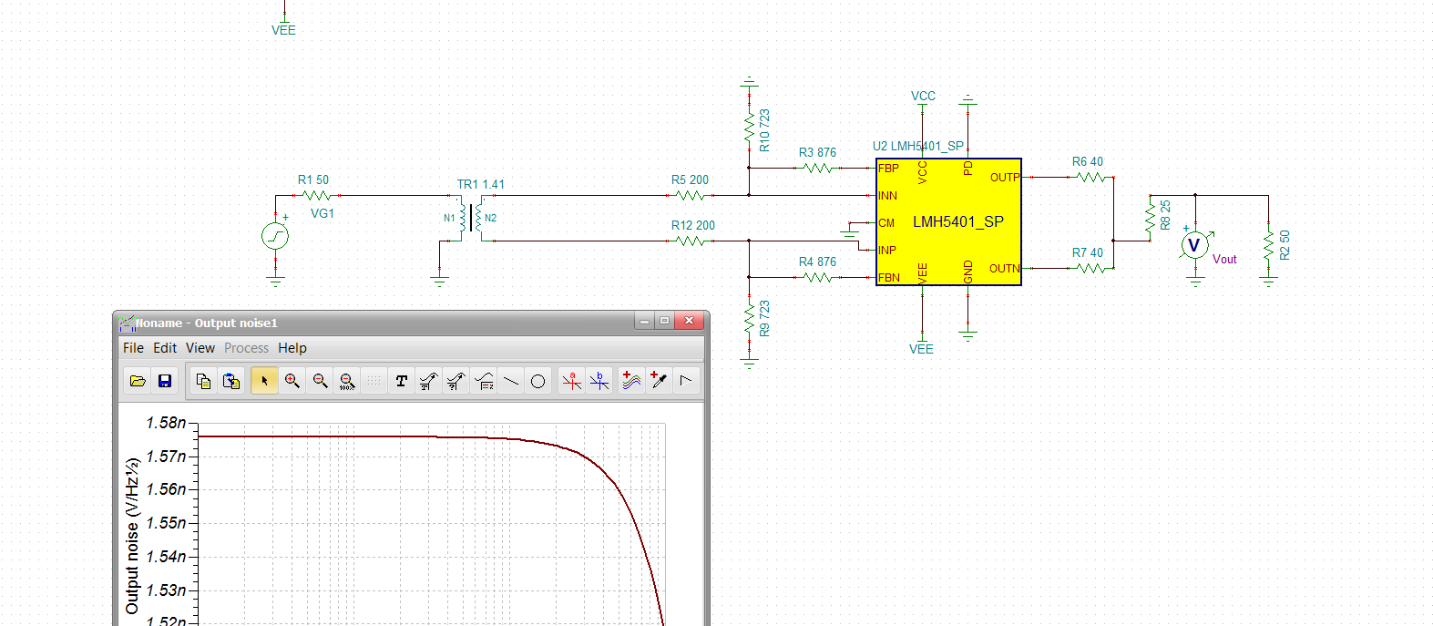
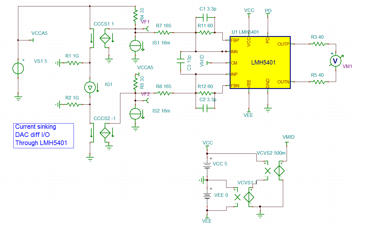
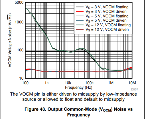
I am using the LMH5401-SP in a differential to single ended configuration. The measured noise figure was much greater than predicted from the noise models. The issue appears to be due to common mode output noise. What is the common mode output noise supposed to be? With the circuit below I measured 6.4nV/sqrt(Hz) of common mode output noise (doubley terminated measurement into 50 ohms). TINA predicts ~1.6nV/sqrt(Hz).

Thanks,

Shawn

  • Morning Shawn, 

    Could not see your attachment, a TINA file is best if possible, The little paperclip in the bar above allows you to insert files. 

    The CM noise becomes differential through feedback divider ratio mismatch. I have noticed some errors in both PDS CM noise and then modeling (have not looked recently at this FDA, but others). Physically, the output CM noise should be highest if the pin is floated. Cap there or driven should be better. 

    Not sure what you are trying to do, but the FDA (and this one particularly) can deliver pretty good noise figure in either the balun input or active balun configuration. Active balun is slightly lower NF with slightly degraded even order HD, whereas the balun input is still pretty good on NF with lower even order HD. 

  • Hi Michael,

    Good morning! The TINA file is attached. The noise was measured using an LNA + spectrum analyzer with an overall noise figure of 1dB. With a 15dB ENR noise diode connected through a transformer to the input resulted in less then a 0.1dB increase in output noise when the common mode noise was measured using the TINA circuit which indicated that the resistors are well matched around the circuit. The common mode voltage is connected to a ground plane, the circuit is powered off +/-2.5VDC. Both supplies are filtered with LDO's followed by pi filter networks. The capacitors used in those networks are the feed through type and placed adjacent to all 4 power pins and connected directly to the ground plane. We tested a similar circuit on the LMH5401 eval board and found the same result; a high noise figure when measured single ended, and the expected noise figure when measured differentially. 

    Thanks,

    Shawn

    DAC_AMP_AC.TSC

  • Very nice summary Shawn, Your schematic looks ok except I think the impedance match might be off - that looks to be a 1:1.41 turns or 1:2 ohms ratio which would suggest two 100ohm inputs for match - differential input impedance is just the sum of the two Rg's.Those R's to ground only increase the Noise gain hurting NF. 

    I ran your sim for output spot noise, looks way too low for what I know is inside there - reflected back up through the match, this is about 3.2nV CM noise at internal output pins. I cannot find any spec or plot in the datasheet, so not sure what the modeling guy was trying to match to. What you measure for CM noise is likely more correct and it looks like you are doing it correctly. 

    The model header does not claim CM noise modelled, 

    I did try to work through the NF equation for the balun input FDA a few times, here is the latest - matches bench so I have some confident in it. 

    THis is a 2 part article, saying EDN wrote ? Not so, I did these, 

    https://www.edn.com/accurately-predict-measured-noise-figures-for-transformer-coupled-differential-amplifiers-part-1-of-2/

  • Hi Michael,

    Thanks for the link to the article. When this circuit is used in the real system the output comes from a DAC which has internal 50 ohm pullups to +3.3V. The circuit has to be DC coupled to the DAC and have an output common mode voltage of 0V. Dropping the input resistors to 50 ohms would have pulled the DAC outside it's output compliance range. So a trade off was made between the impedance match and common mode compliance range.

    Thanks,

    Shawn

  • Thanks Shawn, 

    I think I may have worked on this problem at one time - are you in Phoenix? 

    So obviously your last comments mix things up a lot, if you need to be DC coupled, why is the balun in there? Perhaps the CM on the DAC needs DC consideration on the DAC pins, but the signal itself is AC coupled through the balun? 

  • Hi Michael,

    I am in Baltimore. Sorry to make this more confusing than it needs to be. We built the board without the $17,000.00 FPGA which contains the DAC to verify everything else works as expected. The transformer was added to the board verify the op-amp circuit works as expected.

    Thanks,

    Shawn

  • No, yours is a different project but yes, what a problem to have those $17k FPGA lying around. 

    So, the input side of your validation schematic looks a bit off, but that is not your question - your question was CM noise - probably not modelled right and as far as I can tell not described in the datasheet. 

    I did do quite a lot of complementary DAC output interface design in the course of the THS3217 and THS3491 developments - there are a couple of reference designs that use the LMH5401 in that app as well if you have not seen them. Listed at this link, 

    scroll down on this page to reference designs, 

    http://www.ti.com/product/LMH5401/toolssoftware

  • Hi Michael,

    Do you know what the output common mode noise should be just due to the op-amp itself?

    If you have an alternate circuit in particular which maintains the 100 ohm differential input impedance, keeps output common mode voltage at the DAC with 50 ohm pullups to +3.3V above 2.7V, has and output common mode voltage of 0 V, and stays within the common mode input voltage of the LMH5401-SP, and maintains the same gain and bandwidth of the current design and is DC coupled I would love to see it.

    Thanks,

    Shawn

  • Morning Shawn, 

    I do not have the expected output CM noise for the LMH5401 - you appear to have measured it, so I guess that is it. 

    I do know the CM loop is current feedback based in the LMH5401 (kind of unique) and had kind of abysmal DC drift vs most FDA's, that might also imply higher noise there - but again CM noise should not get into a well design signal chain. 

    So your test ckt is quite removed from you application ckt it seems. I think you are trying to do a ground centered DC coupled diff output with +/-2.5V supplies?

    The FDA does pretty well level shifting things into range with that output CM loop and that will simulate quite nicely - as a start (since this comes up so often) here is a I/O range article on CFA and FDA - the VFA was the prior article #1, 

    https://www.planetanalog.com/input-and-output-voltage-range-issues-for-high-speed-cfas-and-fdas-insight-2/

    Let me know if you need a pdf of this to see the schematics and tables, this site is migrating platforms and breaking links kind of steadily. 

  • Also Shawn, I found an earlier DC coupled current sinking DAC to diff out with the LMH5401 TINA file - not set up how you want it but a good start (single 5V supply design using an E2V DAC). You can adjust this to your needs. The signal is that IG1 generating complementary inputs from a DC centerpoint with 1/2 the tail currents on each side - running a slow DC square wave will show you where the input pins a moving. 

    Current sinking DAC through LMH5401.TSC

  • Hi Michael,

    It would be nice if TI would update the TINA model and/or the data sheet to indicate the common mode noise. Thanks for the links to the article, I was able to see the figures. I was unable to open the TINA file, if you could send me a picture of the schematic that would be great.

    Thanks,

    Shawn

  • No doubt better data in the datasheet and model would be useful, this is only one of several misses in the FDA models on CM noise. 

    I saved and sent that file as a V9 version as you had sent, should have opened for you, but in the meantime, here is a picture, 

  • Hi Michael,

    Thanks for sending the picture! This is essentially the same circuit I currently have, the only difference is that I added a pull down resistor from INN to VEE and another pull down resistor form INP to VEE so that I can use to trim the DC offsets and adjust the input common mode.

    Thanks,

    Shawn

  • You bet Shawn, 

    Well then you are on the right track, keep in mind those pulldown resistor increase the noise gain slightly impairing output noise. Still not sure why output CM noise should be of much concern? Normally not, but in some audio work I was doing the very high 1/f noise down at 2Hz can become problematic once feedback ratio mismatch is considered. 

  • Hi Michael,

    I agree that the resistors will result in higher noise; we can always not populate them. The reason we are concerned about the common mode noise is because we are performing a differential to single ended conversion with the op-amp. The stage after the op-amp is single ended and there isn't a replacement for the second stage that offers differential inputs. The 1/f noise may end up being an issue for this system as well. 

    Thanks for all your help, I really appreciate it!

    Thanks,

    Shawn

  • Well yes Shawn, 

    Anything following this stage will have a CMRR that will try to reject the CM noise with mixed success (over frequency) and that can be a concern. 

    1. Your balancing resistors might give a nominal diff output zeroing, but not over temp unless this is a cal loop. 

    2. output CM 1/f noise is yet another poorly modelled (described) element. 

    I was recently mystified comparing the "measured" output CM for the MCP6D11 FDA vs the finally released THS4561 - the driven input CM noise plot is pretty remarkable (suspect) on the latter, 

    MCP6D11 CM noise plot - at 2Hz, this could get a little scary - 

    And then the THS4561 where the driven input noise looks almost chopper like in flatness to low F - interesting, 

  • Hi Michael,

    Since our second stage is single ended it has no common mode rejection and thus the common mode noise is an issue.

    I don't know how the op-amp offset varies over temperature. It seemed to me that zeroing it at one temperature could possibly lower it over all temperatures but it could also make it worse I suppose. Does TINA model the temperature dependence of the offset? We can compensate the system digitally for the offset vs temperature, but we want to minimize the nominal offset in the hardware.

    The common mode noise when driven vs non-driving is interesting. For my case the pin is tied to ground which corresponds to driven I guess. Perhaps there is an optimum source impedance that minimizes the output common mode noise.

    Thanks,

    Shawn

  • the 2nd stage is single ended - you are perhaps using only one side of the FDA output? That not only bring CM noise into play but will yield much worse even order harmonics as you have lost the balance cancelling those terms.