This thread has been locked.

If you have a related question, please click the "Ask a related question" button in the top right corner. The newly created question will be automatically linked to this question.

INA190: Layout issues

Part Number: INA190
Other Parts Discussed in Thread: TLV61046A, , TLV61046

Good morning.

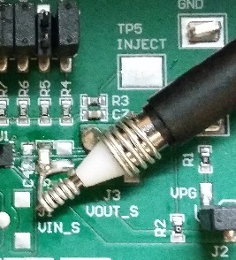
I have an urgent request for layout review of a second run on a PCB.  I initially posted to the power forum as I have a TLV61046A (boost) converter on my board and although helpful, the suggestion was to post again where I may receive overall layout recommendations/help on noise related issues.  Is there someone at TI whom I can connect with where I can share my design files (both original PCB and proposed next spin) as well as captured waveform files of what I am seeing?

Sincerely,

Steve

  • Hello Steve,

    Welcome to the amplifier's forum. If you want, you can send images of the INA190 layout/schematic and oscilloscope waveforms in this thread or through a private message directly to my account. Please also provide a description of the problem and what you expect to be seeing. 

    Sincerely,

    Peter

  • Peter.

    I messaged you privately.  Can you please acknowledge that you received all the schematics, gerber (pdf) and zip files.

    Thanks

    Steve

  • Hey Steve,

    I was able to successfully download your files. Thank you. I am reviewing them now.

    I also am reaching out to other support group located hosting at this forum:

    https://e2e.ti.com/support/power-management/f/196

    Best,

    Peter

  • Peter....

    This is great I look forward to hearing any and all recommendations you may suggest!

    Thanks so much for the assistance

    Steve

  • Hi Steve,

    Peter reached out to me and I would like to try and help.
    I will continue evaluating the files sent to me by Peter, however I am curious if you could send me a picture of your measurement technique for the plots.

    Switching converters are known to produce large amounts of radiated emissions through the switching magnetics, like the boost inductor in your design.  I am hoping that the wires you are using to make your measurements are far enough away (and small) from the boost inductor L1 such that the radiated emission from it is not interfering with the measurement.

    If you can please send a photograph or two of how you made your measurements, we can review and move on from there.

    You may already be familiar with this technique, but I want to pass it along anyway in case you (or others reading this post) can benefit from seeing it.
    An example of a high fidelity measurement technique is shown below.
    The loop area between the probe tip and GND is very small, which provides a high quality measurement and accurately captures high frequency content.
    It may be sufficient to move your wires and probes as far away from L1 as possible, or we may need a measurement like this, or we may need to troubleshoot the issue in another way.

    Thanks,

    - Stephen

  • Stephen....

    I'm not gonna lie....at this end I do have loops and wires as I had to connect a demo board to my design.  I have taken measurements with a traditional ground lead (yes the long wire) for the readings but I then switched to the technique you are using with a lead wrapped around the ground as in your picture but this did not make a difference for me.  I recognize that the signals aren't the cleanest however and that some of this could very well be due to technique, however with that said I would like to know if you see any layout things that concern you.  Are you seeing waveform anomalies that indicate there are issues?  If so please indicate on what waveforms and where and I will go back and try and make cleaner measurements with respect to those points.......

    Sincerely,

    Steve

  • Hi Steve,

    I've had some more time to review the work products you sent over.
    I have some additional questions to make sure I understand the circuitry and layout correctly.

    Boost Converter Operation
    1. Is the boost converter still operating in burst mode?

    Component Placement
    I don't expect this to make a huge difference, but going forward I would swap the placement of C21 and R8.
    This reduces the loop area just a bit for C21.

    PCB Layout
    1. In the PCB drawing file, is it correct to say that page 1 = silkscreen, page 2 = layer one (with components), page 3 = bottom layer?
    So 2 layer board total.
    2. Is layer 2 a GND plane?
    3. Does layer 1 have a copper pour connected to GND?
    4. I am not certain if this will make an impact or not, but it's something to consider. 
    The LDO output trace is thin, and routes through the PCB slot and directly underneath R10.
    If there is noise on this trace, it will capacitively couple into R10 through the plane layers and would seemingly show up as common mode noise, not differential mode noise.  The differential mode filter installed on the board would not be as effective against this common mode noise.  The INA190 will gain up the noise by >80dB as you have calculated.

    Measurements
    1. Can you confirm where in the schematic you are measuring?  I was assuming the output of the LDO, but I reread the email and I'm have lost where it says the node being measured.
    2. In the TPS7A4701 FD measurement, there is a spur around 5kHz and none around 40kHz.
    In the time domain measurement, you can see the low frequency modulation (5kHz) with noise around 40kHz riding on it. 
    There is also lower frequency content in the TD measurement, but we will ignore that for now.
    I think a fresh FD and TD measurement, with pictures of the measurement technique, may be needed, as the FD and TD plots for the TPS7A4701 contradict each other.  Keep the wires located as far away as possible from the boost inductor, and twist any wires placed onto the board.  If you cannot send these images through E2E, please send them to Peter and he can forward them to me - and we can work this through email.

    Thanks,

    - Stephen

  • Stephen...

    Boost Converter Operation:

    Correct Burst Mode...Load is only about 4.5mA - 5mA.

    Component Placement:

    I am using the "ANY-OUT" programming function...R8 will be 0 ohms with C21 as DNP.


    PCB Layout:

    Page 1 is Top Silk and Top solder mask (to show pads)....Page 2 is top copper (1 ounce) with Cu pours.  The large pours (2 of them) are tied to GND.....Page 3 is bottom copper (1 ounce) with the Cu pours tied to GND also.  There are NO planes here just 2 layers with both being majority of GND net.

    I am looking into if I can swap pins 2 and 3 to accommodate NOT running LDO output under R10....That trace doesn't seem thin to me...It is 20 mils and only carries 5mA.  Am I missing something?

    Please note the cut in the ground pours and the remaining copper on the top side that connects the two ground pours.  I purposefully choked these connections down so to try and keep the HF wanting to not circulate up where the amplifier section was.

    Measurement:

    The files START with a naming convention according to the net name that is being measured (please refer to the schematics)....For instance "Signal", "Sensor", etc.  The spur at 5kHz is the input signal from the sensor.  It is valid (actual signal is 5450Hz).... That is correct the TPS7A4701 FD does NOT exhibit 40kHz noise BUT the LT1761 FD plot does....I believe the TPS7A4701 is doing a good job wrt removing the burst frequency of the TLV61046 (this burst frequency is around 40kHz at the light load I described (~5mA).  What I do not understand is WHY the TD between the LT and TPS graphs looks the same.  I would have guessed that if the FD plot is good then the TD plot would have been good UNLESS there is something else going on due to oscillations, etc. 

    Thanks

    Steve

  • Stephen...

    Please allow me to connect with you outside the forum and I will share pics and pdfs of scope shots.

    Thanks

    Steve

  • Hi Steve,

    I have sent you a TI "friend request" so you can see my work email and directly send me this data.

    Thanks,

    - Stephen

  • Hi Steve,

    I received your files and am reviewing them now.
    Regarding the "thin trace" - it is not thin, I think when I wrote that I had your small board on my large monitor, and sometimes you lose track of the size of things.  It is sized just fine to carry the current.

    These plots look different to me than the previous set that I was reviewing.
    In these plots there does not look to be a contradiction in the TD vs FD plots. 
    What I mean is, you can see the ~40kHz spur in both plots.

    So what we need to do next is to determine how much ripple is going into the LDO input and how much exists on the output.
    For this test, I would measure right on the EVM.
    I would also do this with the shaker table off, that way we will only see the effect of the circuitry without the additional noise from the table.
    If you measure Vin and Vout with this approach, we can do the math to determine if the PSRR is providing the attenuation we would expect it to.

    Thanks,

    - Stephen

  • Hey Steve,

    I did some SPICE simulations and can see that the INA190 oscillating is not a concern. Your signal chain should work.

    I was speaking with Stephen and we have some general debugging step we highly suggest you take.

    1. Clean up all measurements. Use Coax cables
    2. Reduce wire lengths and remove all hanging wires near inductors.
    3. Re-check measurements
      1. All voltage measurements using Coax cables.
    4. Check/measure the 5V rail.
      1. This could be getting noise fed back from U4, which would add significant error to entire signal chain.
      2. Try using a separate 5V source
        1. De-populate R27 or L3 in order to remove this as possible variable.
        2. If this works, consider using another linear reg after U3 to provide the 5V rail.
    5. Try replacing U4 with something that does not use boost mode since this is noise sensitive application.
    6. When measuring the “Signal” (voltage across R10), use a differential probe with coax/shield cables.

    Sincerely,

    Peter

  • Based upon communication through direct messaging, it seems there is a path forward in addressing the issues of this post.

    Best,

    Peter