This thread has been locked.

If you have a related question, please click the "Ask a related question" button in the top right corner. The newly created question will be automatically linked to this question.

TLV2172: How to adjust gain and DC smooth in Full wave precision Rectifier

Part Number: TLV2172
Other Parts Discussed in Thread: TLV172, TINA-TI, XTR115, TLV9002, XTR111

Hello,

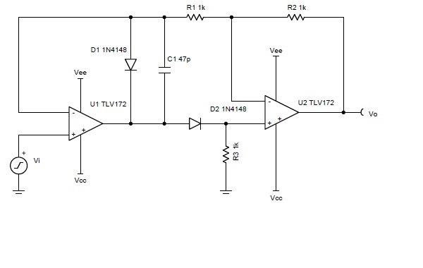
I am designing Full wave precision  rectifier circuit to convert AC to DC. I just plan to use (TLV172 based) below circuit to convert AC to DC with scaling. 

I have two question here.

1.  How do i adjust gain here. If i adjust R1 & R2 , will the gain be adjusted?

2. My input is Vi (AC/50HZ). If i use 10uf or 22uf capacitor at output(VO), will it be converted to pure DC signals?

Regards,

Winiston.P

  • Hi Winiston,

    why not running a TINA-TI simulation by yourself?

    Kai

  • Hello Winiston,

    1) This will unbalance the matching of the positive and negative gains.

    2) A direct capacitance will be problematic.

    Are you interested in the peak, average, or RMS voltage? In other words, can the sine quality be ignored.

  • Hi Ronald,

    1.  I want to increase the gain maximum of 5. How to increase the gain ?

    2. Yes. Sine quality can be ignored. The output of TLV172 (VOUT) is uni directional signal (pulsated) and I want to convert it into  pure DC signal for feeding as analog signal to XTR115.

     In legacy bridge rectifier, if we add capacitor at the output of bridge rectifier , the full wave uni directional signal will be converted to DC signal.

    In the same way, If i use precision rectifier like TLV172, and add capacitor at the output side of TLV172, Will it be convert into DC signal ?

    Ultimately , I want to convert, output of TLV172 to DC signal and feed it to XTR115.

    Regards,

    Winiston.P

  • Hi kai,

    I have download TINA, How to simulate ? Can you give some hint ?

    Regards,

    Winiston.P

  • Hi Winiston,

    has this thread to do with this one?

    What is wrong with the circuit I developed for you there?

    Kai

  • Hi Kai,

    Nothing wrong in that design . Our project runs on time limited. So i have to make 100% working pcb in one shot. This one i made as back up plan.  More over, that (TLV9002) is half wave rectifier. It may be given lesser DC level when i convert from uni directional pulsated signal to pure DC signal.

    I still have a doubt , how to convert uni directional signal output (TLV9002 out) to pure DC signal? If i add 22uf capacitor at the output of TLV9002, Will it convert to pure DC signal ?

    Regards,

    Winiston.P

  • Hi Kai,

    Thanks for your quick response.Please find your attached Simulation circuit.

    3583.arockia_xtr115_1.TSC

    If I give VG1 is less than 300mv.  VF1 & VF4 are not linear. VF1 is starting from 0.8V and VF4 is starting from 500mV.  So We can not convert low voltage signal.

    I need a linear curve starting from 50mV.  It means that if  CT output is in the range of 25mV or 50mV , i should get corresponding output from VF1 or VF4.

    Can you suggest me the method or fine tune components value in your design to achieve from 25mV or 50mV ?

    Regards,

    Winiston.P

  • Hi Winiston,

    according to figure 1 of datasheet of XTR115, for an output signal of 4...20mA the current "IIN" flowing into pin 2 of XTR115 must change from 40µA to 200µA.

    Keeping in mind that "IIN" is "AM1" in my simulation, my circuit provides exactly that:

    arockia_xtr115_2.TSC

    Kai

  • Winiston,

    What is the desired transfer function? For example [0mVpeak to 1Vpeak] at CT converted to  [4mA to 20mA] after XTR

  • Hi Kai,

    Thanks for detailed description. I also simulated in TINA. It works well. But i want to understand the following queries.

    1. You added 40µA as offset or in other words Scale starts from 40µA at AM1  . How did you add this offset or Which resistor is doing this activity ?

    2. Now scale starting from  40µA to 200µA  when we give 0-2V at VG1... If i want to make same scale 40µA to 200µA with the input(VG1) of 0-1V,  How do i achieve?

    3. As per XTR115 datasheet, what ever current consumes either in Vref or Vreg will get added at the output as offset. For example, TLV9002S consumes 6mA, XTR115 is able to drive current starting from 6mA to 20mA...So current consumes by TLV9002S is also accountable here. How much current TLV9002S consumes?

    4. Please find attached full application circuit. I replaced ground to Iret and made the schematic as per your guideline. If i simulate now, AM2(output of XTR115) always gives greater than 19mA irrespective of input voltage(VG1)... and AM1(output of TLV9002S) is not linear at low voltage. For example, If i provide 100mV at the VG1,   AM1 suppose to give 48uA . But it gives 60uA... But greater than 1V input(VG1), the output of AM1 is linear. Can you justify the mistake.. It works in linear without XTR115 section.

    Kai_XTR115_1.TSC

    If you justify above clarification, it will be very much helpful to me. Will this simulation output also be equal to Practical one ?

    Thanks,

    Winiston.P


  • Hi Ronald,

    Yes, You right. desired transfer function is 0mVpeak to 1Vpeak at CT converted to  [4mA to 20mA] after XTR.

    Regards,

    Winiston.P

  • Winiston,

    I did not want to depend of the XTR input resistance always being 2.5k , so I drive the XTR with a current source. The second op amp is an offset (by 40uA) current source (gain 160uA/V). The first op amp is a half wave and more importantly unidirectional current rectifier (like a old school diode half wave, without the forward voltage drop). Two op amps can do the job. Most of the components on the CT side are just to improve tolerance to EOS/ESD as I expect CT signal may come from a connector.

    CT to Isource.TSC

  • Thank you very much Ronald to analyse my scenario and created schematic.

    I want to clarify your and Kai design.

    1. How do i adjust Offset or  Which resister do offset activity ?

    2. How do i adjust current source gain ?

    3. Shall I use this design to voltage input activity like XTR111 based design too ?

    Regards

    Winiston.P

  • Winiston,

    U3 is a negative peak detector. R2 C1 sets peak response time (and affects U3 loop stability). R3 & C1 set the decay time and voltage ripple. Gain is 1.

    U1 formula is quite complicated. IOUT  = (VIN * ( 1+ R11/R12 ) - Vreg * R11/R12 - ( Vreg - VIN) /R12*R5) / -R5 (all voltages are relative to VREF, including Vreg)

    VIN = 0 yields 40uA, VIN = -1 yields 200uA.  (adjust R5 to set gain[0V to -1V]; adjust R11 to get 40uA at VIN=0; repeat if needed)

    XTR111 has a voltage input, so my circuit would need to be changed to support a voltage output instead of a current output,

  • Hi Ronald,

    Thank for your time and consideration.

    It exactly matches for my application. I need voltage output also to feed to XTR111. I hope that  Kai(refer mail conversation) circuit meets voltage and current source.  Can you develop voltage output to interface XTR111 ? I need 4-20 mA or 0-20mA and 0-5V output from XTR111 also. I already referred XTR111 Eval circuit. It has the provision to select 0-20mA or 4-20mA and 0-5V output. I should have voltage output circuit to feed to XTR111. 

    Can your simulated circuit tally with practical one?

    Note: XTR111 circuit also used in CT 

    Regards,

    Winiston.P

  • Winiston,

    Please provide the math equation(s) or input/output ranges with CT voltage as input and XTR111 input voltage as the required output.

    For example, the previous solution was 0mVpeak to 1Vpeak at CT converted to  [40uA to 200uA] at input of XTR

  • Ronald,

    CT converted output is same as 0mVpeak to 1Vpeak and  0-5V DC at input of XTR111.

    Note : I need 0-20mA  or 0-5V at XTR111 output, I hope that I should provide 0-5V DC at XTR111 input. Please clarify.

    Regards,

    Winiston. P

  • Ronald,

    CT converted output is same as 0mVpeak to 1Vpeak and 0-5V DC at input of XTR111.

    Note: I need 0-20mA and 0-5V DC at XTR111 output side. I hope that I need 0-5V DC at input of XTR111. Please clarify.

    Regards,

    Winiston. P

  • Hi Kai,

    Will your  circuit works as Voltage source ? I mean to say that, It i feed your circuit output to input of XTR111 , will it work?

    Regards,
    Winiston.P

  • Hi Winiston,

    we have given you everything you need to finish the project by yourself and to make the circuit successfully work. I really like to help when a problem occurs. But I cannot do the whole development work for you. This goes far beyond the scope of this forum.

    This is the circuit I proposed for the XTR115:

    The offset can be adjusted by the help of R9, the gain by R12.

    The XTR115 and XTR111 are different in nearly every respect. And what works for the XTR115 need not to work for the XTR111 and vice versa. Please study the datasheets!

    For the XTR111 I would give this scheme a try:

    arockia_xtr111.TSC

    But some points have to be considered:

    The OPAmp cannot fully reach the supply rails. For the positive supply rail this can be overcome by increasing the supply voltage a bit. The XTR111 allows this. But the XTR111 no longer provides a reference voltage like the XTR115. So, you would need to create the bias voltage at midsupply by another method.

    Kai

  • Winiston,

    Quote "Note: I need 0-20mA and 0-5V DC at XTR111 output side. I hope that I need 0-5V DC at input of XTR111. Please clarify.".  XTR provides an output current, it will not output 0 to 5V (unless the load is a specific value)

    Is the 4mA minimum no longer a requirement? It is difficult to design a circuit when the requirements keep changing.

  • Hi Ronald,

    Thanks.

    Ronald:   XTR provides an output current, it will not output 0 to 5V (unless the load is a specific value)

    Winiston Reply :   XTR111 output load is 249 ohm. So with respect to 249 ohm load, voltage needs to vary  from 0-5V.

    Ronald: Is the 4mA minimum no longer a requirement? It is difficult to design a circuit when the requirements keep changing.

    Winiston Reply : Dear Ronald, Still our requirement of XTR111 is 4-20mA and 0-5V output only . Since I can give some voltage offset on XTR111 input by using voltage divider. I mentioned as 0-20mA.  We can connect 249 ohm resistor at XTR111 load side to drive 0-5V.  It is good for me if you design either of below two design.

    1. 0-20mA and 0-5V  at output load 249 ohm

    2. 4-20mA and 0-5V  at output load 249 ohm

    Regards,

    Winiston.P

  • Hi Kai,

    Thanks for your all the effort. Sorry if i trouble you. We may use this design for multiple application. So adjusting gain and offset  is required. More over Current driven and voltage driven are also required. So only I asked. This is actually a portion of my project. I only have doubt on this rectification portion. Thanks for clearing all queries and designing. Once the product is developed, i will give a feedback. Thanks for supporting me.

    Regards,
    Winiston.P

  • I'll try to do this one by the end of the week.

    1. 0-20mA and 0-5V  at output load 249 ohm

  • Ronald,

    Yes. You are right. Your decision is welcome.

    Regards,
    Winiston.P

  • Winiston,

    Amplifier is below. Peak detector (gain = 1). Amplifier Gain = 5 so [0V to 5V] going to XTR111 pin 6 (input)

    RSET is 2.49k. IOUT is 10*VIN/2.49k ; [0mA to 20mA] out of XTR111. Your load is 249 ohms * [0mA to 20 mA] = 0V to 5V

    CT (gain 5) 0V to 5V.TSC

  • Hi Ronald,

    Thanks for time and guidance. I kept both the circuit and designing PCB . I will give a feedback once it is tested. Thanks.

    Regards,

    Winiston.P

  • Hi Kai,

    I made a design based on your current driving circuit to XTR115. It works well. Thanks for your continues support.

    Regards,

    Winiston.P

  • Hi Ron,

    I checked your above design with all components mounted. It works good. Thanks for your great support and guidance.

    Regards,

    Winiston.P

  • Winiston,

    I'm glad that you are having success. 

  • You are welcome :-)

    Kai