This thread has been locked.

If you have a related question, please click the "Ask a related question" button in the top right corner. The newly created question will be automatically linked to this question.

LM358: LM358 : phase Margin Simulation and pull-up register qeustion

Part Number: LM358

Dear Team,

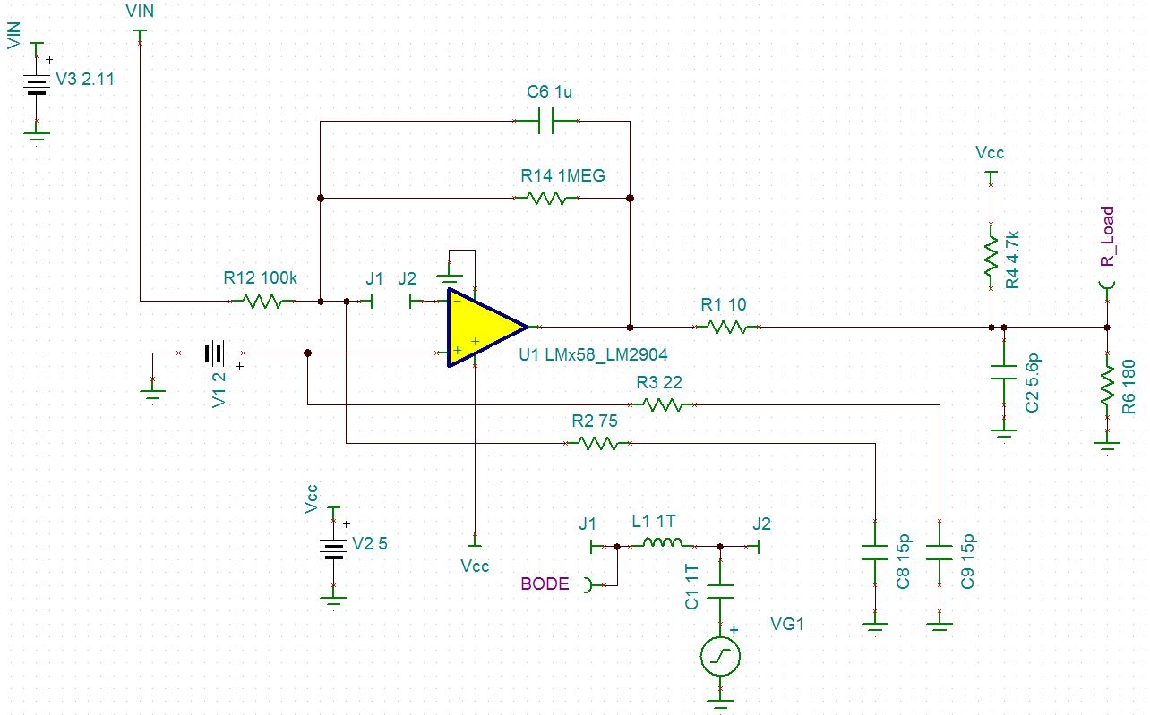
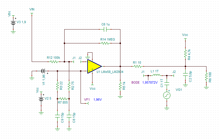
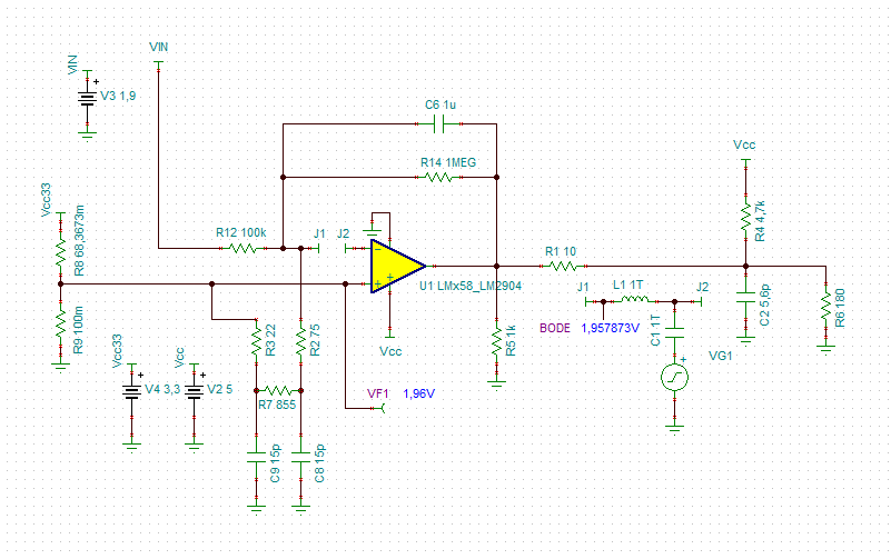
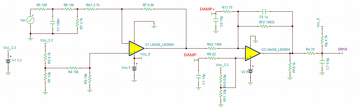
I'm developing a camera iris by completing the LM358.

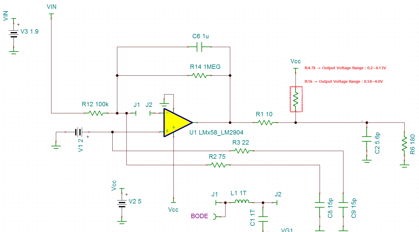
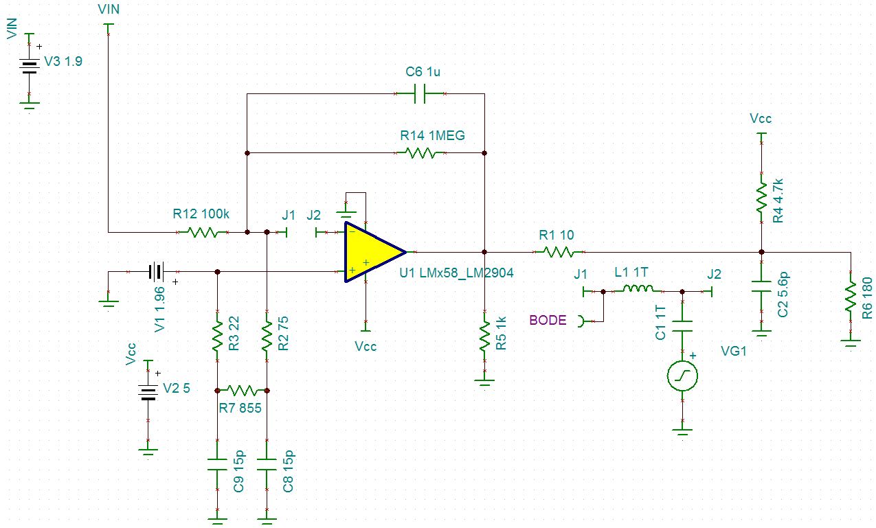
The application part of the LM358 is the motor end of the iris.

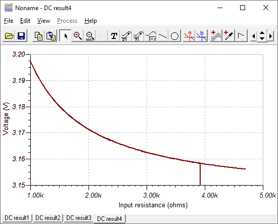
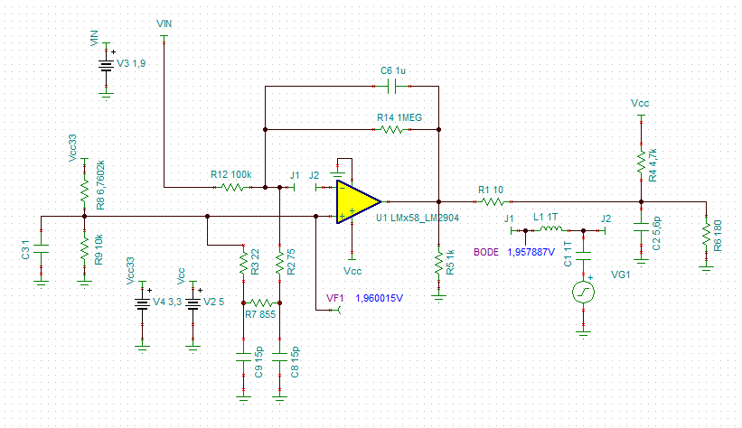
Supply Voltage of LM358 is 5V, and DRIVE,DAMP load Resistance is (DRIVE:200ohm at 20 ℃, DAMP:900ohm at 20 ℃).

I will send you the reference circuit.

0383.DC_IRIS.pdf

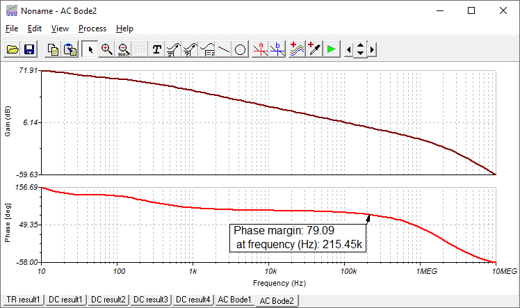
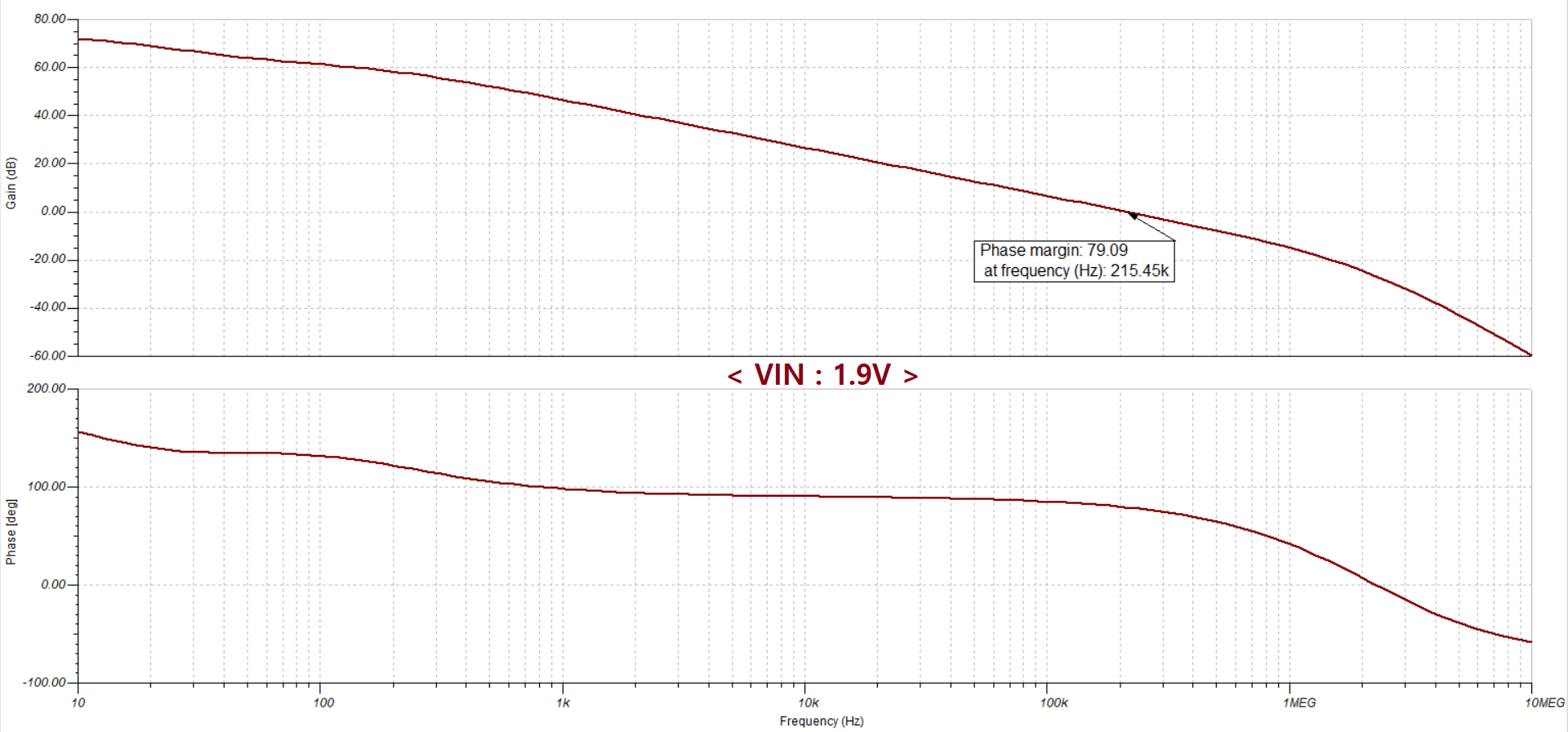
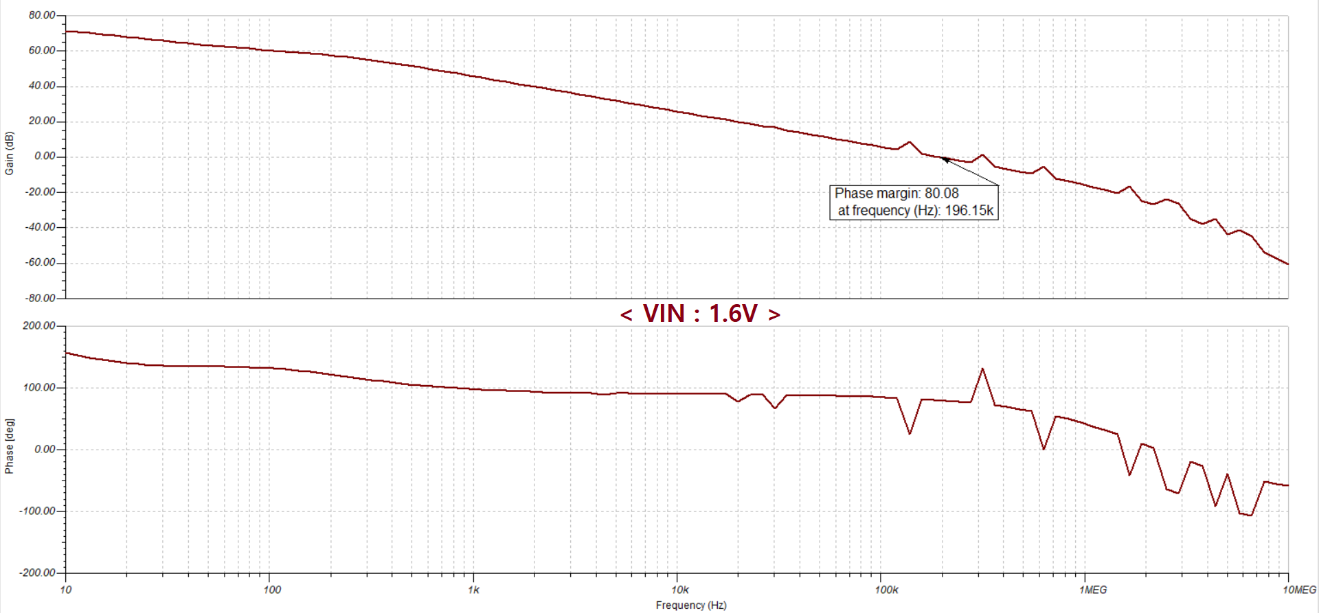
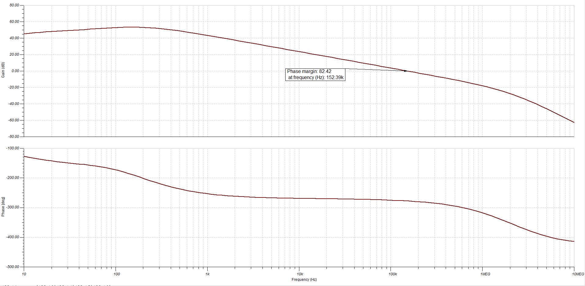
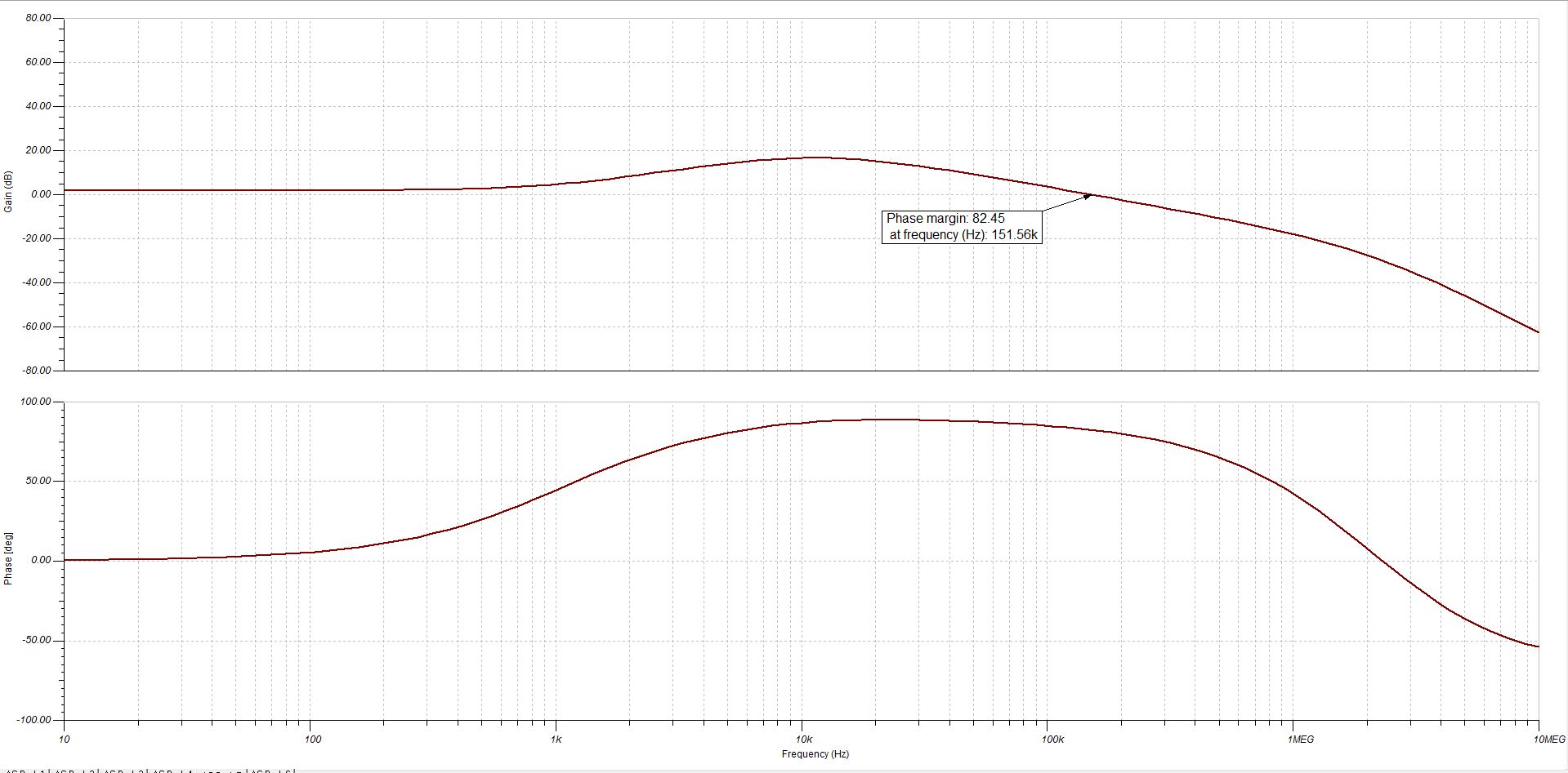
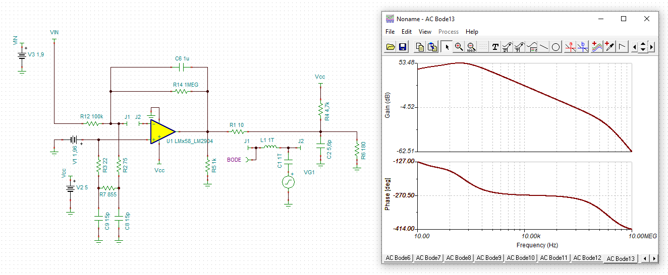
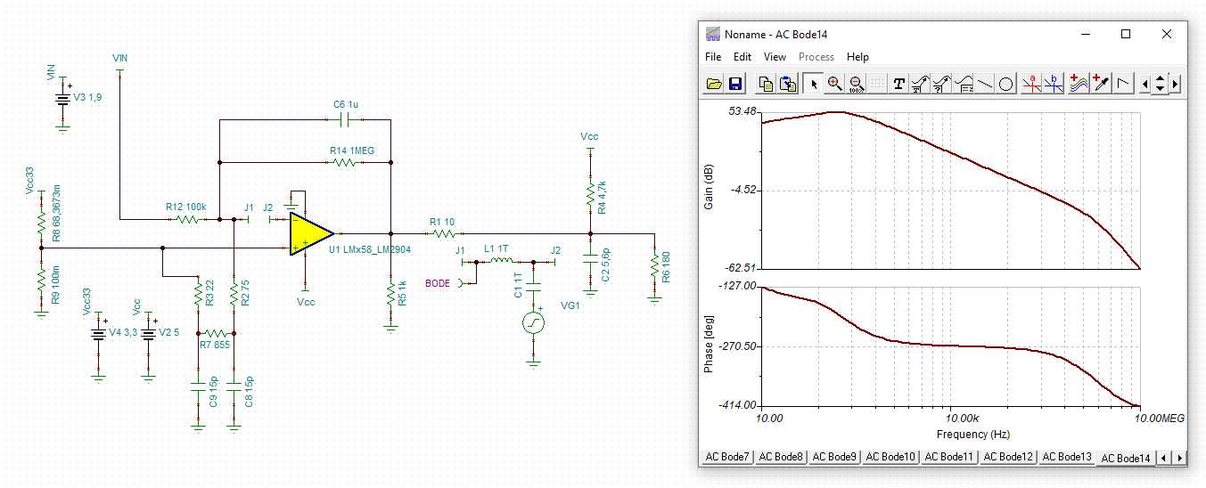
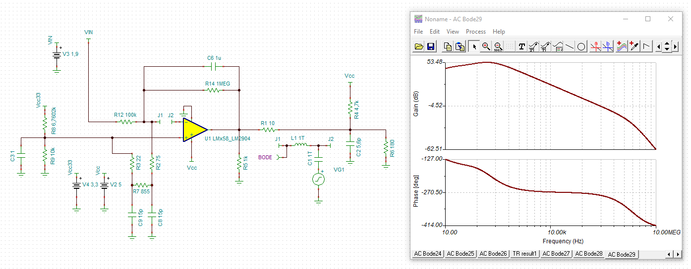
Please review the simulation to be sent.

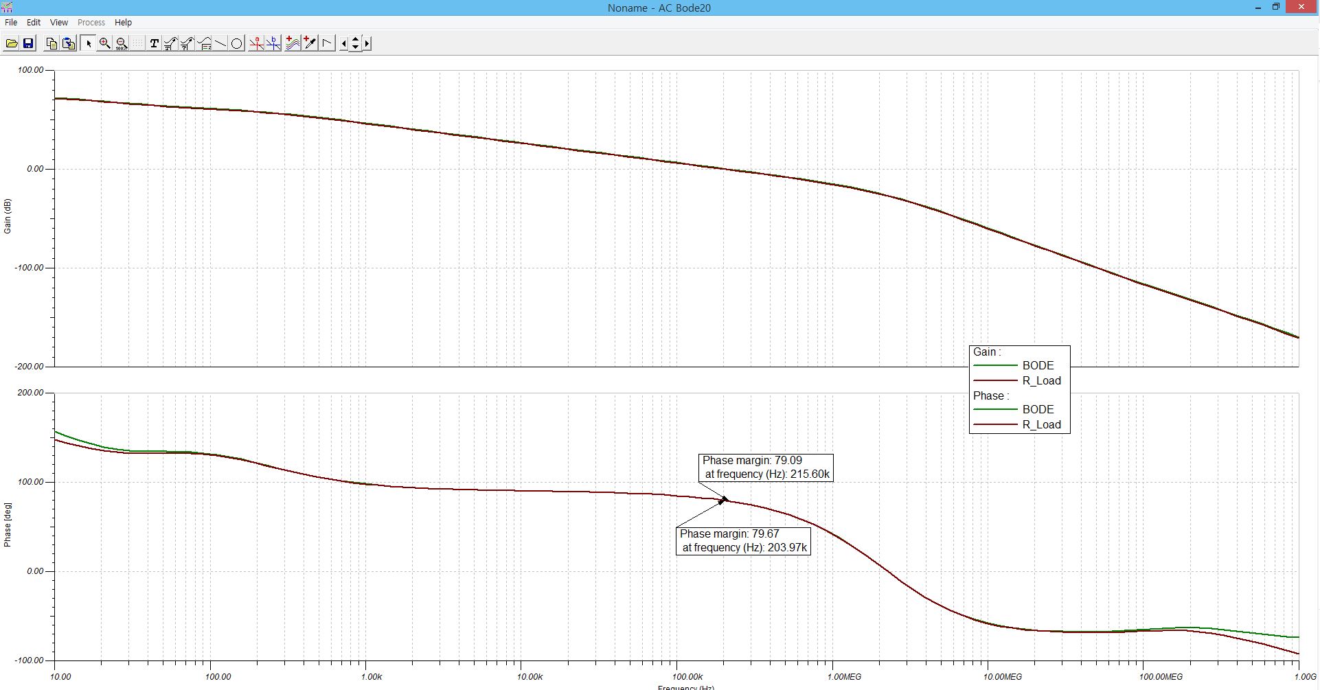
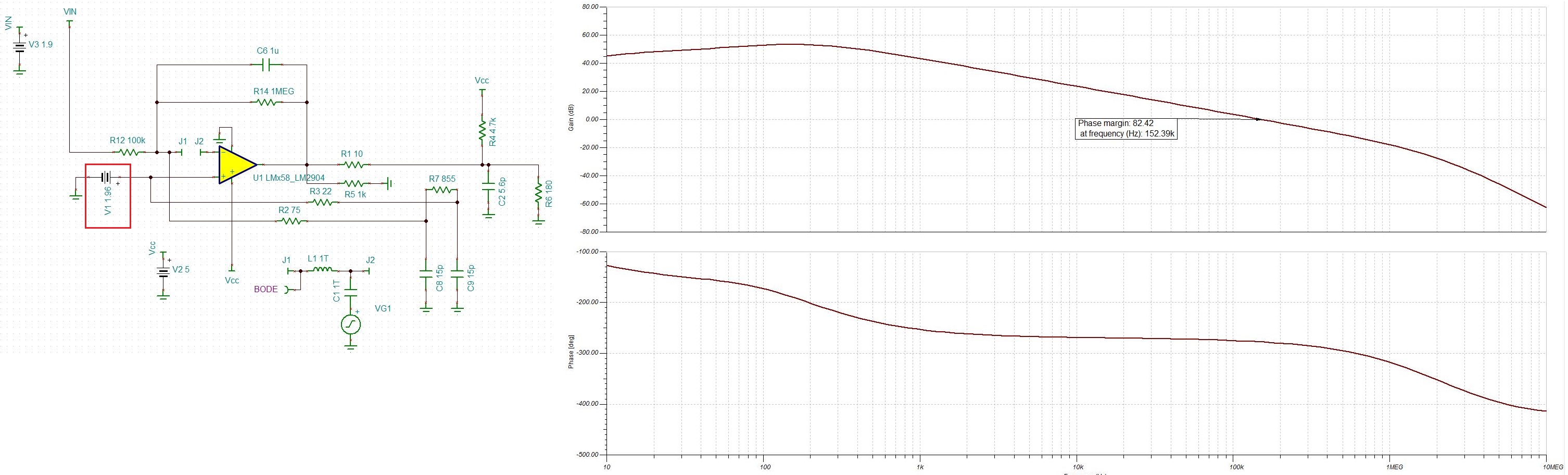
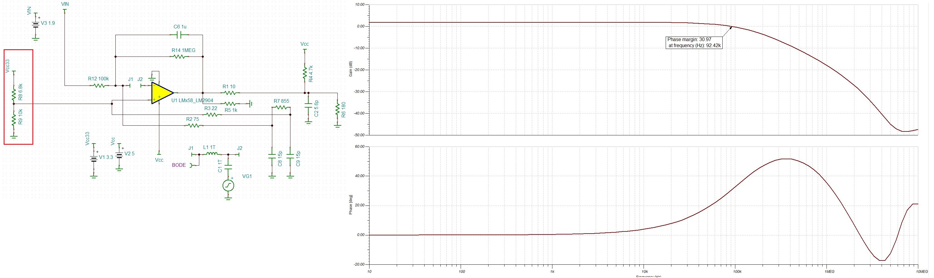
In addition, we request DRIVE Voltage's phase margin simulation for stability of the circuit.

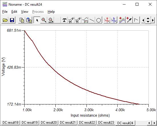
And I have additional questions, there is a 4.7k pull-up resistor on the drive output and 1k pull-down resistor on the secondary op-amp output.

It is judged that it is not insignificant to affect the output voltage because there is a high value resistor. I'm curious about your opinion.

Finally, do you think Ro (10ohm) is necessary for the operation of the circuit?

I asked the manufacturer of the ref circuit, but it did not give a definite answer.

Please tell me if you have any material you need.

Please reply. Thank you.

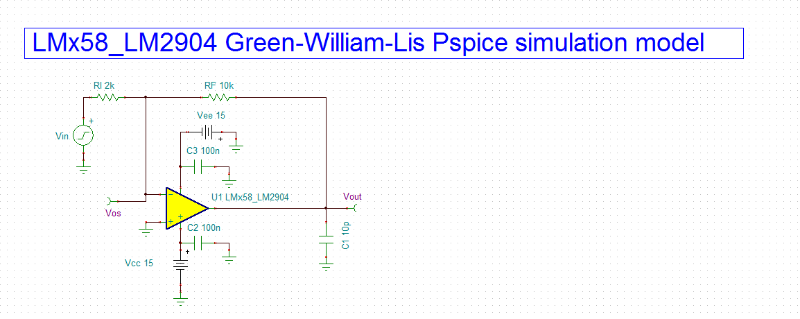
< TINA Simulation - using LM358>

LM358_Simulation_RefDesign.TSC

  • Hello Si Yoon Kim,

    The DAMP = 900 ohm, assuming it is resistive (and floating) at DC, creates over 1000V/V gain in U2 amplifier. This also amplifies input offset voltage which could be partially but not total corrected by IRIS PWM if that happens in the loop.

    One of the pull resistors might make sense, but using both doesn't make sense to me.

    Here is the circuit with DRIVE and DAMP added.

    LM358_withDamp,Drive.TSC

     I believe a low offset op amp is needed for this application. 

  • Dear Team,

    thank you for your reply. 

    Can I request DRIVE Voltage's phase margin simulation for stability of the circuit?

    Please tell me if you have any material you need. 

    Thank you.

  • Si Yoon Kim,

    Do you have a better model for the DRIVE load or should I just use a 200 ohm resistor?

  • Dear Team,

    DRIVE load (Motor_IRIS) area is the black box part. I think you can just use a 200 ohm resistor.

    Thank you.

  • Dear Team,

    If the circuit is complicated, i will send you separate the secondary circuit.

    Please, measure the Phase margin.

    Thank you.

    DRIVE_OUT_LM358.TSC

  • Si Yoon Kim,

    Here is the result for your circuit 

    Here is the test circuit

    DRIVE_OUT_LM358(PhaseGain).TSC

  • Thank you for your answer.

    I would like to ask about the Phase Margin circuit you sent me.

    1) Actually, the VIN voltage is a signal made by smoothing the PWM signal, so a voltage of 1.6 ~ 2.1V occurs depending on the situation.
    However, at 1.6V, the waveform of the BODE Plot distortion is generated.
    Is it unstable at that voltage? Do I need to make the settings different? What is the cause?

    2) We want to get the phase margin based on RL = 180ohm. V_OUT_BODE is connected to the (-) terminal of OP-AMP. Doesn't matter?
    Also, the DC_Voltage at unit stpe is 7.5V. Is there a reason?

    Thank you always for your reply.

  • Hi Si Yoon,

    1) due to the gain of -10, the circuit will only work for input signals of about 1.9V...2.1V. Exceeding this range will move the output into saturation and the LM358 will no longer work properly.

    2) The DC level of VG1 has no influence because of the DC blocking cap C1.

    Kai

  • Thanks you for your reply.

    I have more questions.

    1) When I connected another output to R_load, I noticed a difference in the low frequency band. Isn't it right to have an output connected to R_Load?

    2) My Questions were that why used 4.7k pull-up resistor and 1k pull-down resistor, you said that only one pull-up resistor is required. Can you tell me in detail why?

    3) Can i ask you Why do you think serial 10 ohms are connected?

    I appreciate you always for your reply.

  • Si Yoon,

    1) When I connected another output to R_load, I noticed a difference in the low frequency band. Isn't it right to have an output connected to R_Load?

    Stability is all bout the feedback loop, so the gain and phase of the loop is important. RLOAD is an important node when forward gain (transfer function) is measured. However this node does not play a (direct) role on loop stability. The output load (on the op amp) indirectly affects the loop  

    2) My Questions were that why used 4.7k pull-up resistor and 1k pull-down resistor, you said that only one pull-up resistor is required. Can you tell me in detail why?

    A pull resistor can make the op amp output current unidirectional which prevents the cross over delay. The pull restor can help improve VOL or VOH (but, not both). See application note  

    3) Can i ask you Why do you think serial 10 ohms are connected?

    10 ohms is a minor help in case of shorts or ESD (electrostatic discharge) or if the output load was a large capacitance. It doesn't seem to be helpful here. 

  • Thanks you for your reply.

    I have some questions about output pull-up resistance.

    1) As an experiment, I connecting Bias + V, -V to 5V and 0V, and then connecting 4.7k pull-up and 1k pull-up to the output, the drive output range was 0.2V ~ 4.13V(pull-up 4.7k) and 0.58V ~ 4V(pull-up 1k). Can I ask you Do you think this improves VOH and VOL?

    2) In addition, the crossover delay mentioned is specified in the design guide as examples, when a sine wave is input and when the load side current alternates.We use the LM358 as a DC input and a DC output. in this case, Crossover Delay occur under our conditions?

    I appreciate you always for your reply.

  • Si Yoon,

    I assure you that those results do not represent actual results. With either pull up (or no pull up) the maximum output (at op amp) will be less than 3.5V

    The minimum output without pull up will be 0V. 
    With a 4.7k pull up the minimum voltage will be about 0.2V
    With a 1k pull up the minimum voltage will be about 0.7V

    For some unknown reason the model is having an issue in this specific application. I have noticed the the new model has issues with a few applications , but works great in other applications. The old model (built into tina library) works well for VOH, but the VOL is too optimistic.

    I highly recommend reading (or re-reading)  the LM358 app note.

  • I saw a comment in this chain that the loading does not get into the LG sim. That is not strictly correct as the open loop output impedance can sometimes strongly interact with the load before the feedback signal heads back to the summing node. For a long time this effect was masked by poor or simplified open loop output impedance models. I did check, and the LM358 has an updated model that includes a much improved Zol. So be sure you are using that one, 

  • I saw a comment in this chain that the loading does not get into the LG sim. That is not strictly correct as the open loop output impedance can sometimes strongly interact with the load before the feedback signal heads back to the summing node. For a long time this effect was masked by poor or simplified open loop output impedance models. I did check, and the LM358 has an updated model that includes a much improved Zol. So be sure you are using that one, 

  • Si Yoon,

    With some effort, I finally got the simulation to work better. Here is the R4 effect on output low. This looks valid.

    Here is the test circuit

    DRIVE_OUT_Servo2.TSC

    Here is output high vs. R4 value. I had to run a hysteresis curve to get the model to unstick

  • Sorry for the late reply.

    The high voltage output is Because part of the circuit was short.

    I'm sorry for the confusion.I understood about pull-up resistance a little bit.

    I have a question in the simulation.

    The results vary depending on the power configuration at Op-AMP (+).

    For example, if connected 1.96V directly (case1) , and if 3.3V is made to 1.96V using a resistor (case2), the phase margin results was different. (R6,R7=Load)

    Can you tell me why the two cases are different?

    I know that the voltage across V + has an effect on the ib of the op-amp, but I don't think it will have a big impact because ib is in nA.

    Or does it affect other resistances?

    I appreciate you always for your reply.

  • Hi Si Yoon Kim,

    it's hard to decipher the component values. Can you post the schematics again, with a better reslution?

    Kai

  • Thanks you for your reply.

    Here it is. These are more convenient to see.

    I will attach TINA Simulation circuits.

    DRIVE_OUT_LM358(PhaseGain)_Devide.TSC

    DRIVE_OUT_LM358(PhaseGain)_DC.TSC

  • Additionally, In the case of 1.9V using 3.3V, adding 100nF 2ea caps in parallel improves the phase margin.


    Can you tell me in detail why?


    Is it good to add for stability in the actual circuit configuration?

    DRIVE_OUT_LM358(PhaseGain)_Divide+cap.TSC

  • Hi Si Yoon Kim,

    it's a difference whether the 1.96V is provided by a voltage source with zero ohm output impedance or a voltage divider with 10k // 6k8 source impedance. "10k // 6k8" means the parallel impedance of 10k and 6k8. If you decrease the voltage divider to very small values, at least theoretically :-), you will get the same results:

    si_lm358.TSC

    si_lm358_1.TSC

    Kai

  • Hi Si Yoon Kim,

    the same is valid, if you mount a filtering cap to the voltage divider. But the source impedance becomes now frequency dependent. If you increase the filtering cap to a very large value, again at least theoretically, then you will get the same results again:

    si_lm358_2.TSC

    Kai