This thread has been locked.

If you have a related question, please click the "Ask a related question" button in the top right corner. The newly created question will be automatically linked to this question.

INA128: The protect circuit design and calculate before the INA128

Part Number: INA128
Other Parts Discussed in Thread: INA828, ADS1246, TINA-TI

I want to use the Zener diode to design the protect circuit for differential input before the INA128. So I try simulate the circuit by using the BZD23-C6V2 to create the VDD(6.5V) and VEE(-6.5V) before the INA128. 

Before simulate the circuit, I don't know it will normally execute. After the simulate the circuit seems can run.

I want to know how to calculate the value of voltage(VF3, VF4) on this circuit.

Do I need use Thevenin's theorem to solve it or any theorem? 

And do anything need to notice if I use the +15V, -15V, zener diode and resistance to create the VDD and VEE?

Best Regards,

Brian. Chou

  • Hi Brian,

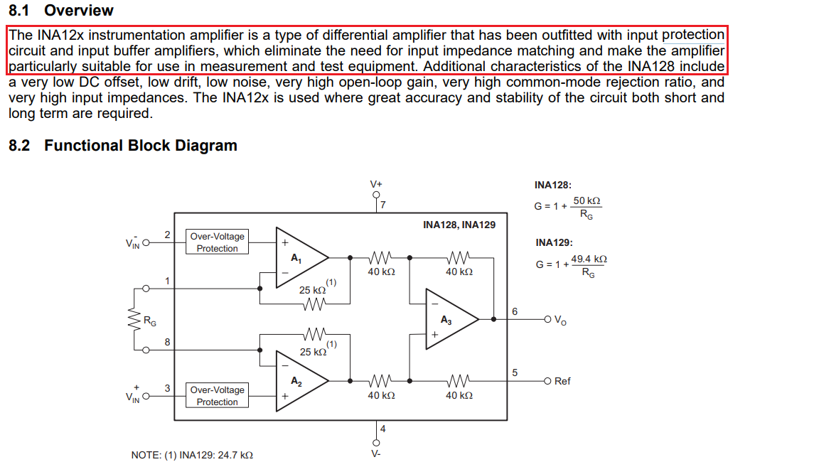
    why do you want to add a protection scheme? The INA128 already contains an input overvoltage protection. External protection diodes, on the other hand, can massively increase the input bias currents and ruin the performance of INA128.

    Also, there's a better variant of INA128 available now, the INA828. See section 7.2 of its datasheet to see how the input overvoltage protection is working.

    Kai

  • Hi Kai,

    Thanks your provide the suggestion about the INA828.

    Because I use the INA128 output connect to the input of ADS1246(VDD: 5V), and I want to limit the output voltage to make sure the voltage under the VDD of ADS1246.

    I see the maximum value of bias current of INA128 about 10nA.

    How much error value( (10nA+BAV99 leakage current) *R1? ) on this circuit before the input of the INA128?

    Besides, I also want to know use this circuit to limit the voltage when the input voltage is differential voltage, how to calculate the value of voltage(VF3, VF4) on this circuit?

    Do I need use Thevenin's theorem or other theorem to solve it? 

    Best Regards,

    Brian. Chou

  • Hi Brian,

    maximum leakage current of BAV99 at 25°C and 25V is 30nA, but considerably increases at higher temperatures. The error voltage of leakage current is 40nA x 3kOhm = 120µV at 25°C. But keep the temperature increase in mind. Taking the ultra low leakage current diode BAV199 will help.

    To calculate VF3/VF4 you make a case decision: Either the BAV99 is conducting, then the voltage VF3/VF4 is clamped to the zener voltage plus one diode's forward voltage drop of BAV99. Or the BAV99 is blocking, then only the leakage current is flowing.

    Kai

  • Hi Brain,

    Thanks for Kai's the weekend support!

    If you have further questions, please let us know.

    Best,

    Raymond

  • Dear Kai, Raymond,

    Thanks help analysis this circuit.

    I still have two question about the clamp circuit.

    Question 1:

    The D1~D4 will replace by the BAV199.

    What should be paid attention to when selecting a diode(Z1, Z2)? 

    Question 2:

    How to calculate the voltage(VF3, VF4) on this differential circuit when using this clamp circuit?

    Best Regrads,

    Brian

  • Hi Brain,

    INA128's voltage rail is +/- 6.5Vdc (the simulated zeners are only +/- 5.75Vdc), and the inputs is protected up to +/-40V. As you know, the input impedance of INA128 or INA828 are extremely high.

    What is your maximum input voltage for the input? Can you tell us more about your application and input impedance before I recommend some kind of input protection scheme? Otherwise, we are not taking advantage of high input impedance features of the part. 

    The input common-mode voltage range is recommended from (V- - 2)V to (V+ -2)V. Outside of the input common-mode voltage range will not produce linear output response. Enclosed in INA128 Tina simulation. 

    INA128 Chou 03102020.TSC

    Best,

    Raymond

  • Hi Brian,

    the exact parameters of the zener diode are not so important because the low junction capacitance of the BAV199, when being reverse biased, will "isolate" the zener diodes noise and the supply voltage noise from the inputs of INA128. More, the junction capacitance of BAV199 will form a capacitive voltage divider in combination with the caps C1...C3 which will drastically suppress the noise of zener diodes and supply voltage.

    I would take a zener diode which needs not too much current for the biasing. There are so called "low current" zener diodes available. And, of course, the zener diode must be able to dissipate the heat caused by the biasing.

    Question 2 is best answered by running a TINA-TI simulation.

    Kai