This thread has been locked.

If you have a related question, please click the "Ask a related question" button in the top right corner. The newly created question will be automatically linked to this question.

Capacitance on op amp causing peaking - fixable?


Hello All,

I have a non inverting amplifier designed using the OPA 727. It is fashioned into a PGA of sorts by switching the feedback resistors with a TI CD4053 analog mux.

It appears that the response to a step input is peaking. According to TI literature, this could be the result of capacitance on the input pins (especially on the inverting pin). I suspect that the capacitance results from the nearby ground plane, leads, and the addition of the analog mux. See the figures below:
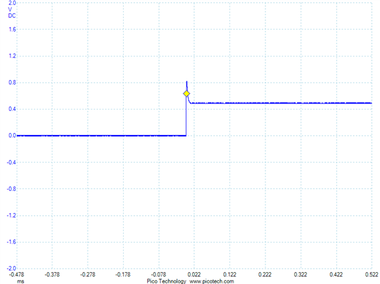
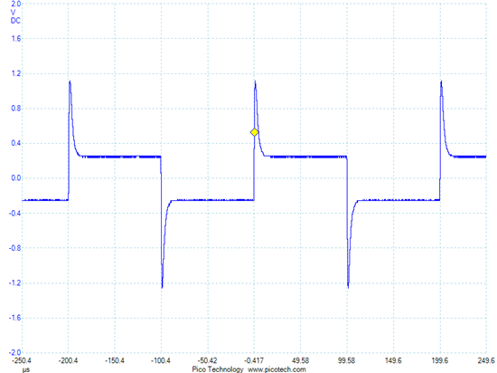

Is there anyway to compensate for this peaking? I know I could re-design, but I would prefer to see if I could add some extra capacitance somewhere to compensate.


Thanks for your input,

Alex

  • Alex,

    In short, the answer is capacitance across the feedback resistor. Without details on the circuit, it's difficult to say what value is required.

    Are you familiar with how a 10x scope probe works? It is a compensated attenuator. R1C1=R2C2. The feedback network to the op amp is an attenuator. The feedback capacitor compensates the attenuator.

    Regards, Bruce.

  • Bruce,

    Thanks for the quick reply. I know about the operation of a compensated attenuator. I was actually using the probe at 1x. I have two lines of though going here:

    1) Perhaps the 1x probe caused extra capacitance loading?

    2) My use of ground planes, etc. caused excessive capacitance on the inverting pin of the amplifier.

    What part of the schematic should I show to help the forum see what's going on? Also, are there any tests I can perform to figure out what my issue is (such as add a resistor to see if the peaking is damped)?

    Thanks,

    Alex

  • Alex,

    I was using the circuit of a 10x probe as an analogy to what is going on in your circuit. Your feedback network to the op amp is like the circuit of a compensated 10x probe.

    First, reduce the capacitance to ground at the op amp's inverting input. If you have gain switching circuitry on this node, this may be difficult. If you have a ground plane under this circuitry, this may be a source of undesirable capacitance.

    Reduce the impedance level of the feedback network. For a given value of capacitance at the inverting input, this pushes the pole out to a higher frequency.

    If the above measures do not sufficiently improve the dynamic performance, add capacitance across the feedback resistor. If you have multiple feedback resistors with different values, different feedback capacitors will be required for each feedback resistor.

    See a discussion on this compensation technique on page 7-16 of this document...

                       http://focus.ti.com/general/docs/lit/getliterature.tsp?literatureNumber=slod006b&fileType=pdf

    You are welcome to attach a diagram for the op amp circuit that is creating a problem. Include all the feedback network circuitry for that op amp and I will try to offer suggestions.

    As a separate matter, it is a good practice to routinely use a 10x probe. This reduces the capacitive loading on the node you are probing to 10pF or less. When and if you use a passive 1x probe (no internal amplifier), be mindful that you could be adding upwards of 100pF load on your probe point, significantly altering the circuit behavior. Active 1x probes (with an internal amplifier) generally have a very low input capacitance and are okay.

    Regards, Bruce

  • Bruce,

    I am using the CD4051 now (not the 4053) as the analog mux to switch the gain. Is there a good way to model its frequency response? I am worried that it will introduce capacitance on the inverting terminal.

    Alex

  • Alex,

    It's really not possible to go deeper into this without a circuit diagram.

    Bruce