This thread has been locked.

If you have a related question, please click the "Ask a related question" button in the top right corner. The newly created question will be automatically linked to this question.

LMH6629: Correct design of a photodiode-TIA setup

Part Number: LMH6629
Other Parts Discussed in Thread: TINA-TI, , OPA725, OPA2743

Hey everyone!

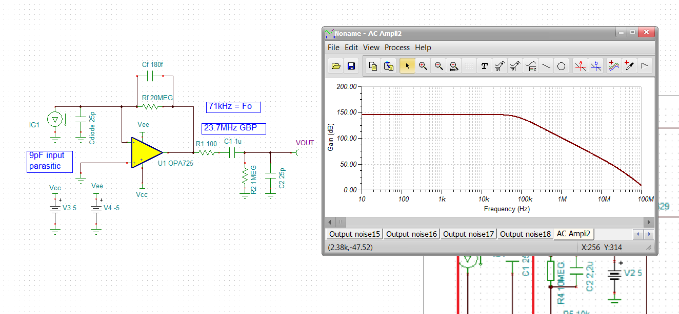
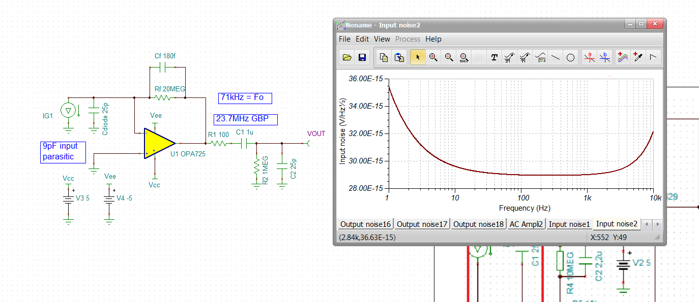
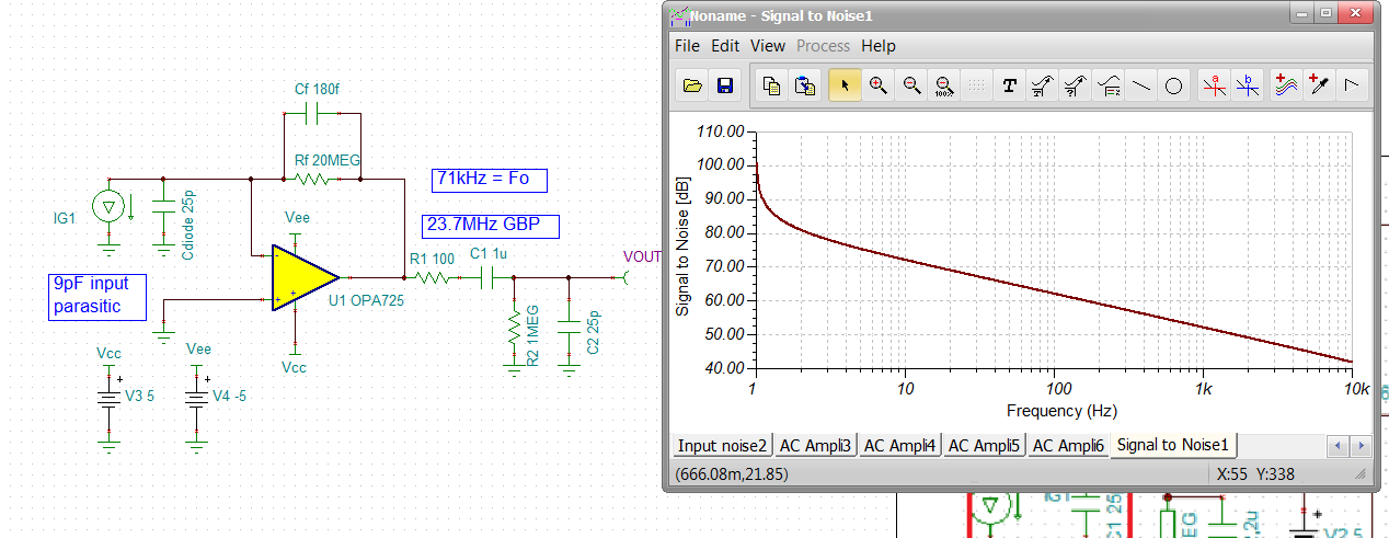
I need to build a first stage amplifier, a transimpedance amplifier, for a photodiode. The diode has a very small suface area, hence I expect a relatively low parallel capacitance but also (due to the application) a very low photocurrent, probably well below 5 nA. The photodiode will be part of a lock-in aplifier based absorption detection system, the modulation frequency of the excitation source (a LED) will be 1.25 kHz. I am looking for a maximum of gain in this first stage, so large feedback resistor values.


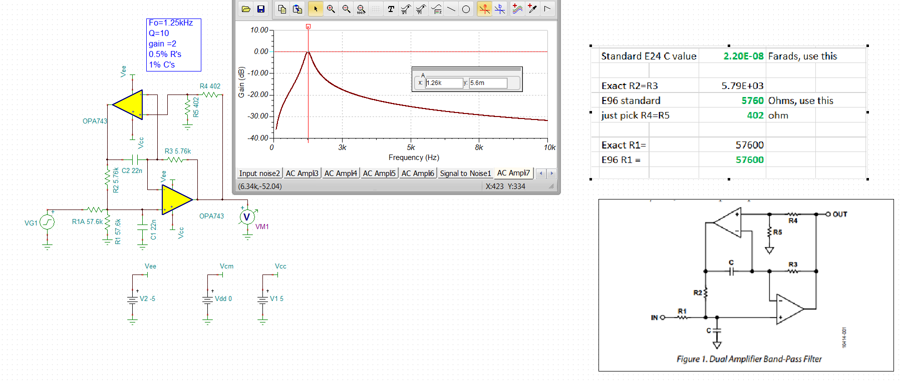
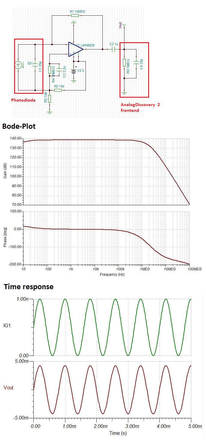
I used TINA-TI to simulate the circuit and I have to admit that I am not really sure what is going on. I tried to use large feedback resistors with 1 MOhm and 10 MOhm resistance. I found that to get a reasonable gain response I need to keep R4, the resistor at the noninverting input, close to the size of the feedback resistor.

1) My questions here: is that because of the input bias current?

2) I understand that the output voltage swing is within ~800 mV of the supply-rails, so I have to shift the level of the noninverting input into this range. Is it better to connect the anode of the photodiode to the same level (here 2.5V through voltage divider formed by R2 & R5) instead to ground as done in the schematics? In the simulation this seams to make no difference...

3) The GBWP of the LMH6629 makes me wonder why the AC simulation suggests a gain close to the expected gain up to frequencies well beyon 10 kHz. Is that realistic? I already doubt the results for 1.25 kHz with 10 MOhm feedback.

I have seen weird effects with a bunch of differen diode/opamp setups until now, so I try to understand all of this a little better instead of just fooling around. Any help or hint is appreciated.

Have a good time and thanks!
Ben

  • Hello Ben,

    1) You may want to use a part other than the LMH6629 in your application. The reason you are seeing better results when adding 10MEG to the non-inverting input is because you are cancelling out your bias current which exceeds your 5nA input greatly. Even if you are able to do this effectively on a real board, the offset current also dominates your input current. Note that the combination of 10MEG at the non-inverting input along with your bias current will also cause you to exceed your common-mode input range.

    You will want to use a FET device which will have lower bias current specs.

    2) It doesn't make much of a difference because of the the DC blocking capacitor you have at the output (C3). You will still need to take the output range specs of the amplifier into consideration, however. In terms of DC, your goal should be to correctly bias your photodiode, in this case you are applying 2.5V at both sides of the photodiode. One way to do this is to apply the positive supply to the cathode of the amplifier, and applying a voltage at the non-inverting so that you get the biasing across the photodiode that you would need. (see the transimpedance amplifier in the first page of the LMH6629 datasheet).

    3) You are using a part with a GBWP way above what is needed for a 1.25 kHz signal. Note that the "gain" in GBWP is not your transimpedance gain but the noise gain of the amplifier. Feedback capacitance is usually added to shape this noise gain so that the device remains stable with the capacitance of the photodiode (Look at page 3 of the this document)

    In summary, I think you should switch to a FET device with a much lower bandwidth. I will move this thread to a colleague that can help you find a more suitable part for your circuit. Please let me know if you have any questions.

    Best,

    Hasan Babiker 

  • Hey Benjamin, 

    Yes, LMH6629 is way too fast for your needs and yes a FET or CMOS input device will help a lot for bias current issues, 

    HEre is a design using the OPA725 - I left this as +/-5V but can adjust it to single supply, The max flat BW you can get is about 70kHz with a 20Mohm R. I chose that because the feedback C solves to about 0.18pF which is about what the parasitic C is on an SMD thick film R. You can add more there if you want and just bandlimit more, You also cannot drive out to a Cload, need that 100ohm series to isolate that. 

    This simulates surprisingly low input spot current noise, 

    Transimpedance design (with some very useful simplifications) is covered here, 

    8081.Transimpedance design flow using high speed op amps.pptx

    You are going to have a lot of output noise, you may want to consider a narrowband filter with some more gain following this stage, 

    Here is the file for this, 

    OPA725 high Zt stageTSC.TSC

  • I took this a little further, adding a 1.25kHz DABP filter following the Zt stage, it will help your SNR but add complexity. Still staying with +/-5V CMOS op amps there, OPA2743. You can adjust this to single 5V with these parts, or use different parts. 

    Original Zt is not bandlimited so its SNR just keeps going down with it wide integrated noise - this SNR is based on a 20mVpp output, 

    right around 1.25kHz, about 50dB SNR, 

    Here is a DABP filter design for 1.25kHz with a Q=10. I got a gain of 1 here, expected 2 but anyway, 

    And then placing this after the transimpedance stage removing those shunt elements to ground, here is the overall gain, 

    And here is the final SNR at the output of the DABP filter stage, a little bit better at 1.25kHz at 54dB, but then stays flatter as the broadband noise is filtered off, 

     here is this two stage file, 

    OPA725 high Zt stage with DABP filter.TSC

  • Hello Hasan,

    thanks a lot for this great, detailed and well explained answer! This clears out all my questions on this topic.

    Regards,
    Ben

  • Hello Michael,

    this is amazing, thank you for your effort! I guess I do understand quite a bit more about amplifiers now, thanks for the linked ppt, too.

    I adapted your design to work with 5V single supply by biasing the non-inverting input to 2.5V. I did not post the entire project as it became fairly complex and I found the other parts to work well, so in order to keep the question simple I just left it out. My total scheme is as follows:

    You mentioned the actual noise response of the system and I guess there are a few things I should mention here. After the TIA a second stage amplifier with variable gain follows, which is then followed by a 4th order bandpass filter at 1.25 kHz. The signal is then digitized by a sound-card system which samples at 44 kHz and 24bit. So I hope the noise won't be to big an issue. As the digitized signal is furthermore fed into a software lock-in amplifier that should also remove noise. I will see how good it will be ...

    As a question: Why did choose a DABP filter? Is there anything particularly special that makes it most suitable in this configuration? I choose a 4th order (2 stage) butterworth filter design.

    Thanks again!
    Ben

  • I thought there was perhaps more to your design, 

    The DABP gives pretty high Q with less variation than the usual MFB or SKF implementations. I always suggest at least 0.5% R's and 1% C's (pretty cheap these days). the next step would be to put your RC tolerance in and run monte-carlo for production spread. The TINA V11 I purchased supports that, the free TI version does not. 

    Here was some earlier work in this area (it was new to me), 

    https://e2e.ti.com/support/amplifiers/f/14/t/794727?tisearch=e2e-sitesearch&keymatch=dabp