This thread has been locked.

If you have a related question, please click the "Ask a related question" button in the top right corner. The newly created question will be automatically linked to this question.

TLV3401: Effect of an input exceeding "VCC + 5"

Part Number: TLV3401
Other Parts Discussed in Thread: TLV3402

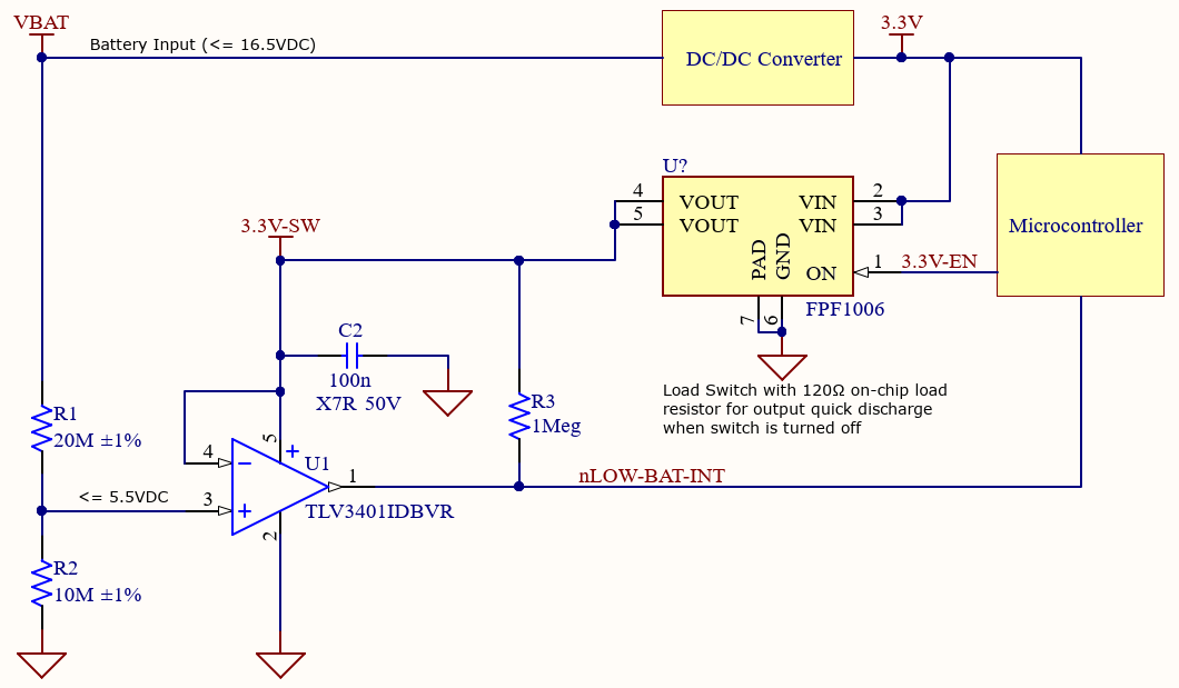
I have a question about exceeding, in a particular way, the absolute maximum rating of the input of the TLV3401. Below is a simplified schematic diagram of a circuit that we made a while back. The TLV3401 is used a detect a low battery voltage based upon a voltage divider of VBAT (1/3 divider). The battery voltage is converted to 3.3V, which powers a microcontroller and a load switch. The microcontroller can enable/disable the switched 3.3V, which powers the comparator (and other circuitry). The load switch has an internal 120ohm discharge resistor, which is present when the switch is turned off.
We have a recent situation where we have a somewhat larger battery voltage than originally assumed. The battery voltage could reach 16.5VDC, and in turn the voltage divider output could reach 5.5VDC. In the event that the switch is powered off (e.g. when the battery is first connected or by control of the uC), VCC of the TLV3401 would be 0VDC, while 5.5V is applied to the “+” input via a 20MegOhm resistor. That voltage exceeds the absolute maximum rating of “VCC + 5”.
Can you tell me more about the internal structure of the TLV3401 and the effect of applying a current-limited 5.5V to the input pin while VCC = 0? Is there a risk of damage, reduced reliability, etc.? I think normally in this situation the ESD diodes would conduct and because the current is limited, it might be ok. However I see this e2e post for the TLV3402 https://e2e.ti.com/support/amplifiers/f/14/t/209321, where it says the input ESD cells are designed to stay off.

  • Jeremy

    I would not expect any long term damage to the device but when the input goes volts above the supply, the input current increases significantly and the performance of the device degrades for as long as the input is volts above VCC.  the +5V over the rail feature is mainly a protection mode, not a functional mode.  So that is why I don't think you will experience any long term negative effect with the condition you describe.

    Chuck

  • Jeremy

    Thanks to resident expert Thomas Kuehl, I believe your questions are answered below.  Thanks Thomas for sharing your knowledge and experience with us.

    Chuck

    “The TLV3402 input circuit is complex and uses two different bipolar differential input pairs. The first pair is effective with a CMV level of 0 V through most of the positive input CMV range. Then, as the positive CMV input level is increased this first differential pair begins to shut down and the other input pair becomes activate. This alternate input stage handles the input levels as the CMV approaches and exceeds the positive supply rail voltage, up to Vcc + 5 V. This design does not rely on any sort of voltage divider when this is accomplished. Also, the input ESD cells are designed to stay off with any of input voltage levels specified even when the positive supply rail voltage is exceeded.”

    “Can you tell me more about the internal structure of the TLV3401 and the effect of applying a current-limited 5.5V to the input pin while VCC = 0? Is there a risk of damage, reduced reliability, etc.? I think normally in this situation the ESD diodes would conduct and because the current is limited, it might be ok.”

    The TLV3401 uses a particular NPN transistor cell that connects from each input and output pin to the (V-) pin. As far as ESD events are concerned the NPN transistor will go into avalanche breakdown if the ESD polarity is positive and high enough in magnitude with respect to V-. If the ESD event polarity is the opposite, negative with respect to V-, the B/E to C diode becomes forward biased. In the case of the positive ESD event the NPN avalanche breakdown won’t occur until the voltage exceeds the TLV3401 absolute maximum supply voltage of 17 V. For a negative ESD event the forward biased junction clamps at a much lower ~0.7 V. Thus, the ESD cell and differential input stage design should be able to stand up to an EOS condition of a magnitude of 16.5 V without damage, although TI doesn’t make any assurances beyond what is covered by the datasheet. The ESD cells are in place to protect for out of circuit ESD events, not in circuit EOS events.

    The real backup protection in your circuit is the 20 Megohm resistor in series with the TLV3401 input. Even if the 16.5 V is applied to the divider and something did turn on dragging the input close to 0 V, the current will be limited to less than 1 uA. That just isn’t enough current flow to damage anything inside the TLV3401 input circuit. Most often we find that a simple series resistor is one of the most effective ways to protect the input of op amps and comparators from moderate EOS events.

    I agree with Chuck. I would not expect any damage or long term degradation of the TLV3401 inputs should the +16.5 V be momentarily applied in the circuit you have shown.

    Regards, Thomas