Because of the holidays, TI E2E™ design support forum responses will be delayed from Dec. 25 through Jan. 2. Thank you for your patience.

This thread has been locked.

If you have a related question, please click the "Ask a related question" button in the top right corner. The newly created question will be automatically linked to this question.

PGA281: PGA281 peformance test method

Part Number: PGA281

Hi Expert,

I am going to use PGA281 in my project and need to verify the performance of PGA281, can you tell me how to test below spec with PGA281EVM? Thank you!

1. Rin and Ro of PGA281

2.CMRR

3.Input offset current, input offset voltage, input bias current

4.Output offset voltage

5.Gain error

6.Capacitive and resistive load drive capability

Best regards!

Rachel

  • Hi Rachel,

    All the measurement you mentioned can be found in the datasheet. Do you want to make these measurement through hardware? or can we do these through simulation. 

    Best,

    Raymond

  • Hi Raymond

    Yes I need to make these measurements through hardware.

    Although these can be found in datasheet, I still need to do a verify through EVM due to project requirement. Can you share these test method? Thank you!

    Rachel

  • Hi Rachel,

    Do you have a particular PGA281 Op Amp configuration that you'd like to test? I am providing you with TI Op Amp training video, and you will figure out how to do these test. If you have questions, please let me know.  

    1a. Rin of PGA281

    I will show you tomorrow. 

    1b. Ro output impedance of PGA281

    https://training.ti.com/modern-op-amps-output-impedance

    2.CMRR

    https://training.ti.com/ti-precision-labs-op-amps-common-mode-rejection?context=1139747-1139745-14685-1138802-669621

    3.Input offset current, input offset voltage, input bias current

    https://training.ti.com/ti-precision-labs-op-amps-vos-and-ib-lab?context=1139747-1139745-14685-1138797-14684

    4.Output offset voltage

    https://training.ti.com/ti-precision-labs-op-amps-vos-and-ib?context=1139747-1139745-14685-1138797-14681

    5.Gain error

    Is there a particular gain setting you have in mind?  I assumed that you are talking about digital gain in PGA281. 

    6.Capacitive and resistive load drive capability

    https://training.ti.com/ti-precision-labs-op-amps-stability-1?context=1139747-1139745-14685-1138805-13848

    https://training.ti.com/ti-precision-labs-op-amps-stability-6?context=1139747-1139745-14685-1138805-13953

    Best,

    Raymond

  • Hi Rachel,

    hmm, why would you want to do this testing? Do you want to hand select a handful of PGA281 for a project?

    Kai

  • Hi Rachel,

    Here are some more information about input impedance and Gain Error measurement of PGA281. You need to be aware that many of measurement in PGA281 requires some specialized test equipment and test environment. It is difficult to reproduce these datasheet results with standard Test Equipment for some of the measurement. 

    1a. Rin of PGA281

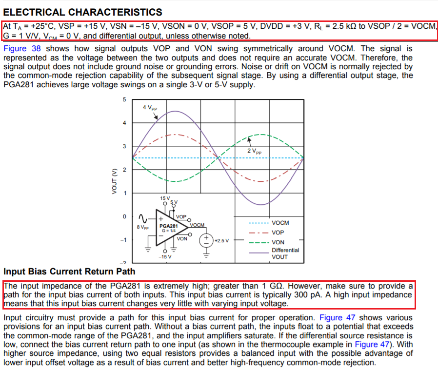
    Configure PGA281 bias circuits as prescribed on top of the each datasheet, see the attached image. Ground IN_N side to ground. Place a precision resistor in series with IN_P, and apply a known sine wave, say 1kHz with certain amplitude at the precision resistor that is in series with IN_P node. The input PGA281 has >1GOhm input impedance. You measure the voltage changes iacross the precision resistor. which is the input current. The ratio of input_Sine_Volt_Amplitude/Delta_I is the input PGA281's input resistance.   

    5. Gain error

    The Gain Error vs.  Gain Setting graph is shown in Figure 9. With the same bench test setup above, you configure PGA281's gain per the table 1. As you input  the sine wave at the differential input, you will measure the differential output swing at the output. The (measured_gain - programmed_gain)/programmed_gain is the percentage error for a given gain setting. 

    If you have questions, please let us know. 

    Best,

    Raymond

  • Hi Raymond,

    Thanks for your reply and detail guidance. I have done some simulation with the methods you give me above, before I go to test bench test, so I can check what  the ideal result should be under these methods. However, I do have some questions during my simulation, and there are many test result much different from datasheet.

    1. Maimum Cap load and R load

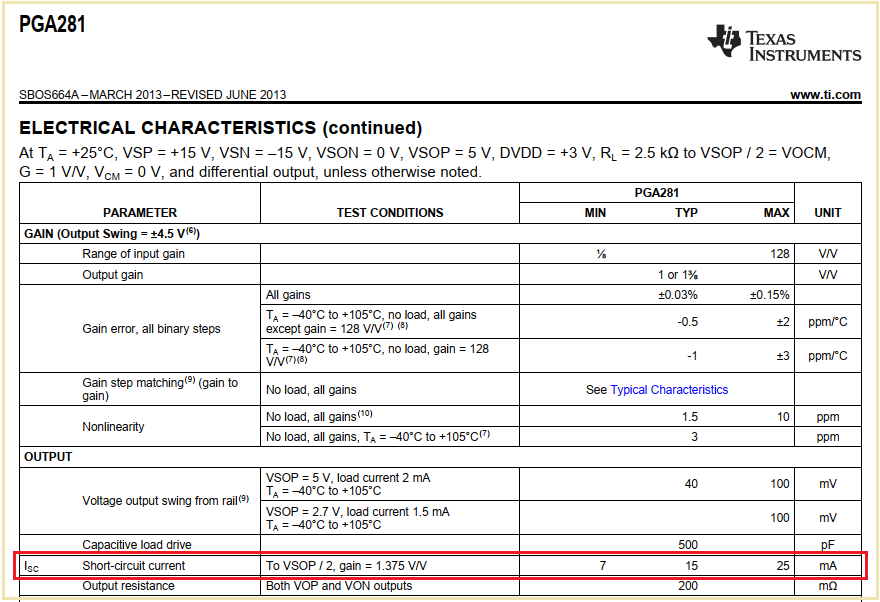
    According to datasheet, the maximum Cload for PGA281 is 500pF,

    1.1 What does 500pF mean(what will happen when CL is larger than 500pF? I think this is the test proof to find the CL ability of PGA281)?

    1.2 Is it means CL above 500pF will get a unstable loop gain(means Phase=180° when LoopGain=0dB )? 

    1.3 How much overshoot in the time domain will be used to define the maximum capacitive load for PGA281?

    1.4 What is  the maximum R load that PGA281 can drive? How to test it?

    2. Vos and Ibias

    I refer to the test method in TI training, but I think it is for OPAMP, not suitable for PGA281(Gain resistors is integrated in chip, I do not know the resistor values).

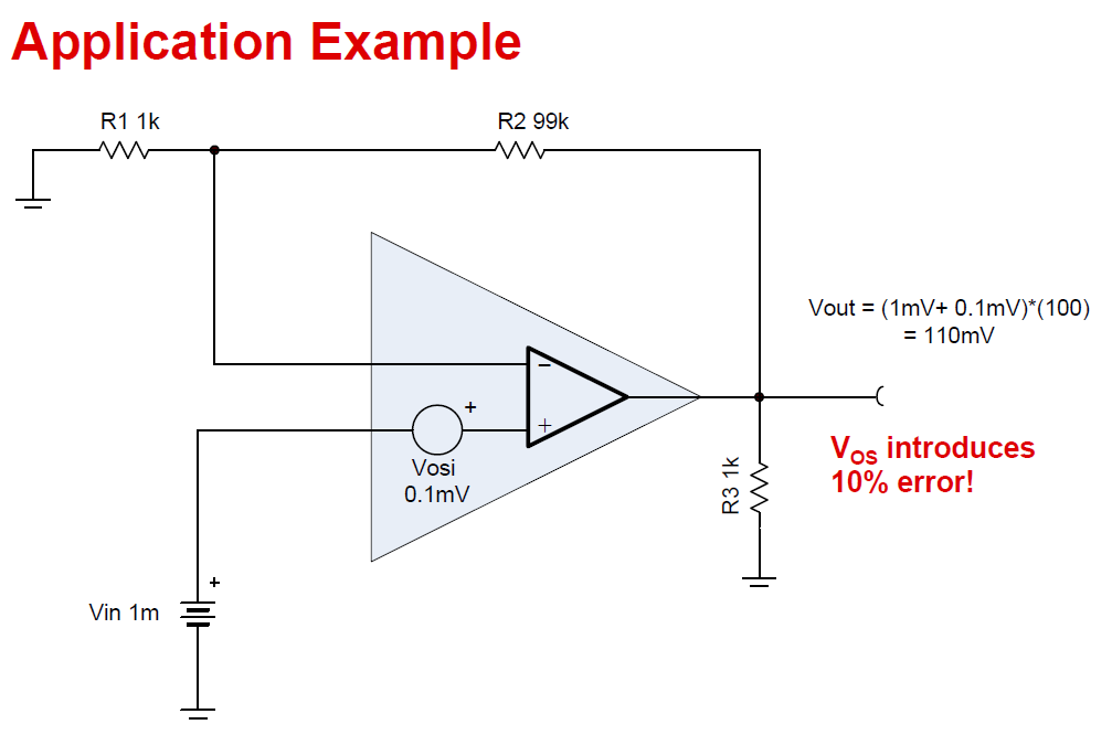
    2.1 For Vos, it need to connect a op-Amp like below picture, and  I will get Vos = Vout/Gain, but this Vout include both Vos and Ibias+ impact, how can I extract the actual effect of Vos? 

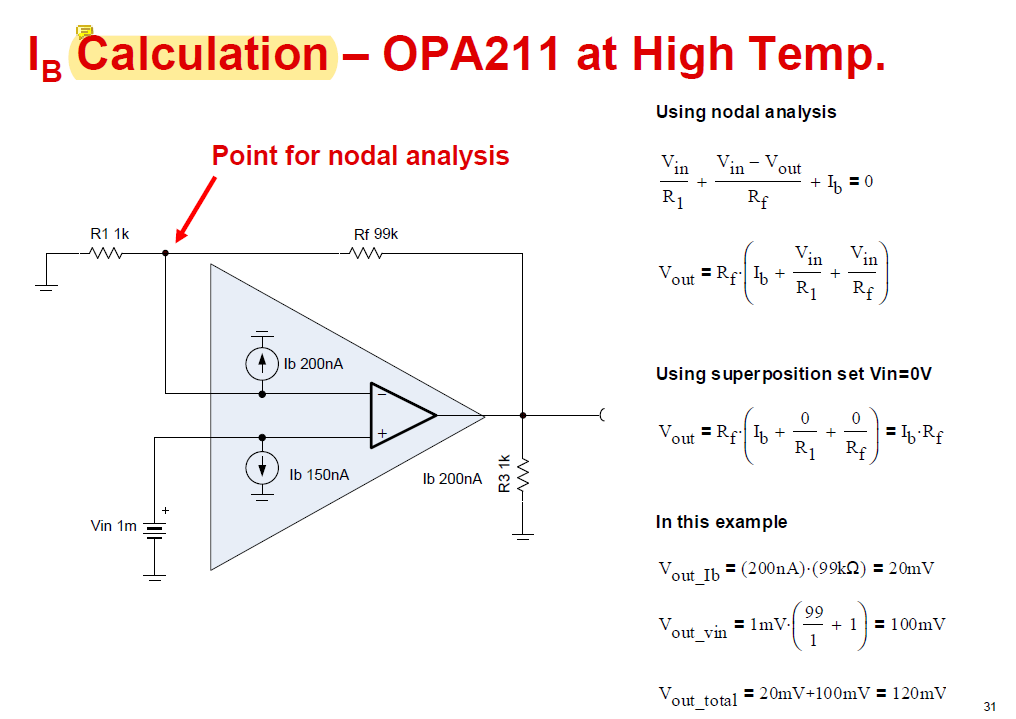
    2.2 For Ibias, it need to connect a op-Amp like below picture, and I will get Ibias- = Vout/ Rf if Vin=0, but for PGA281 integrated all resistors, how can I know Rf value and then get Ibias value?

    3. Rin

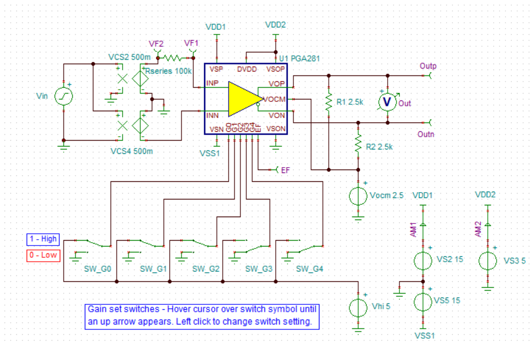
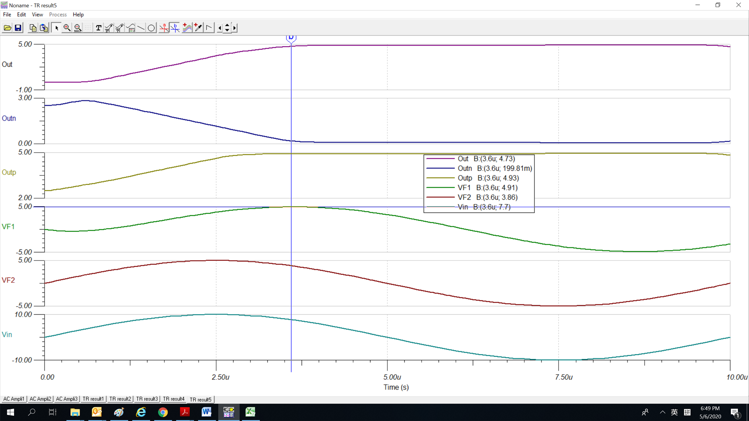
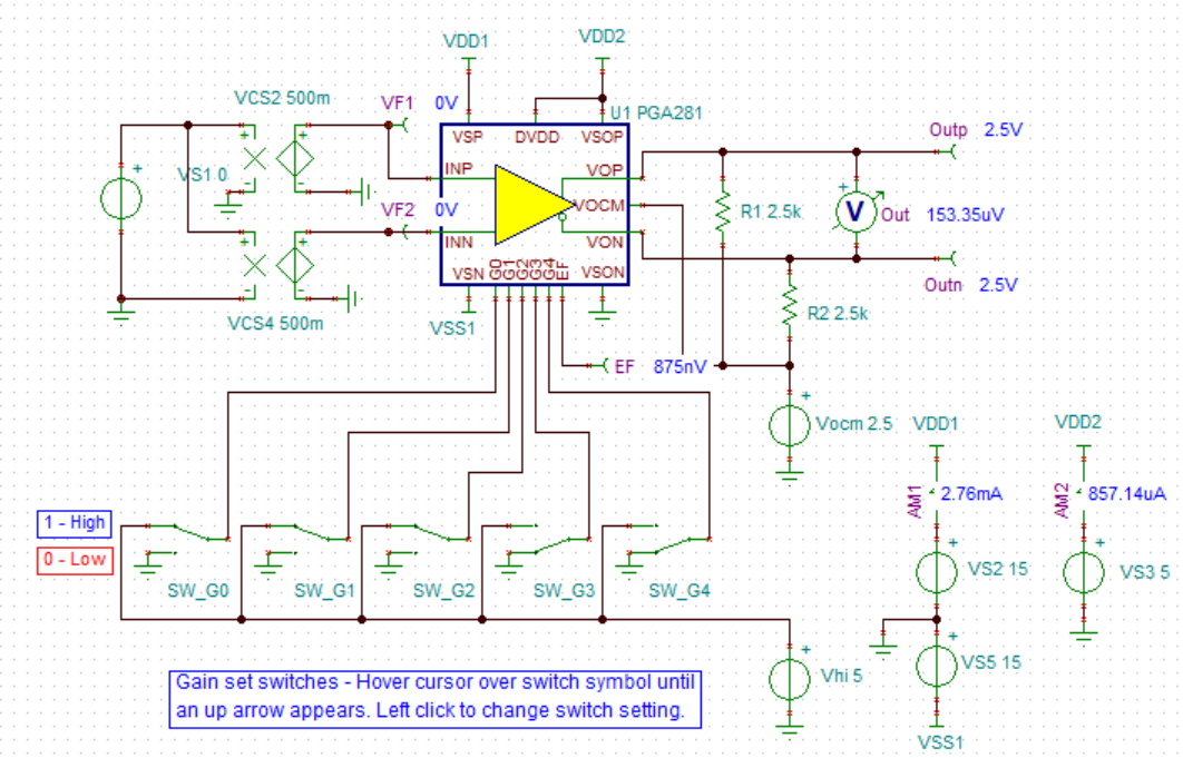
    I simulated with the methods you introduce above, but get dI = (4.91V-3.86V)/100k, Rin = 367.619R, this is much different from datasheet 1MR, below is my circuit and data, anything wrong?

    4.Rout

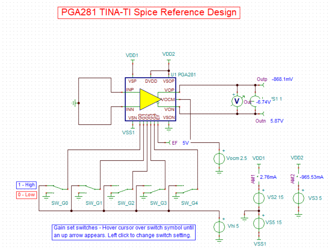
    As PGA281 already integrated close loop resistor network inside, is the output resistor 200mR in datasheet means Close loop Rout?  I use the method in above TI Training link to simulate Rout, place a 1A current source at output, but get Rout = 6.74V/1A = 6.74R not 200mR, below is my circuit and DC data.

    Why so much different from datasheet 200mR?


    5.CMRR

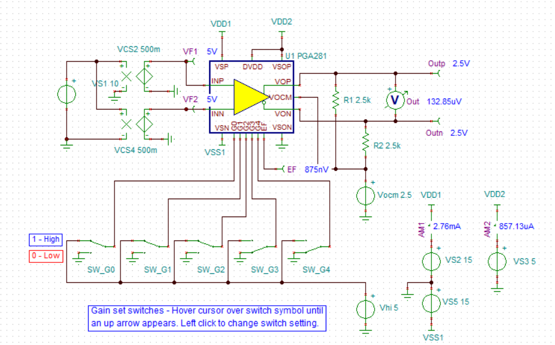
    According to above TI training link, CMRR=dVos/dVcm, so I test Vos at Vcm=0 and Vcm = 10V, but get CMRR = 106dB, this is much far away from datasheet minimum 110dB. Can you tell me if something wrng with my simulation? Below is my circuit.

    Thank you in advance

    Best regards

    Rachel

  • Hi Rachel

    1. Maimum Cap load and R load

    According to datasheet, the maximum Cload for PGA281 is 500pF,

    1.1 What does 500pF mean(what will happen when CL is larger than 500pF? I think this is the test proof to find the CL ability of PGA281)?

    The short-circuit current is ranged from 7-25mA, 15mA being typical. Thus Rload is limited by the output current. I would not recommend to drive more than 3mA, where Rload = Vout_peak/3mA. Most important thing is to calculate the junction temperature and make sure that the Op Amp is not thermally stressed. 

    Op amp does not like to drive capacitive load. It will create instability issues in a closed loop. Please check out the Op Amp Stability Training video in TI site. recommended 500pF load is not guaranteed. It depends on the gain, BW and output load conditions, perhaps even temperature. You are required to check for phase margin before a design is completed. 

    1.2 Is it means CL above 500pF will get a unstable loop gain(means Phase=180° when LoopGain=0dB )? 

    The CL values is not fixed for stability of the circuit analysis. Sometime it is presented in the datasheet as a reference figure, but it is a typical value, and only applicable under the lab circuit test conditions. 

    1.3 How much overshoot in the time domain will be used to define the maximum capacitive load for PGA281?

    Overshoot circuit rule in the training video is a rule of thumb for stability analysis(stability estimation). It is assumed that the op amp rolls off at -20dB/decade with Q equals approx. 1. There are many exceptions for overshoot in the time domain rules. It will be always good to check the phase margins at unity gain BW.  

    1.4 What is  the maximum R load that PGA281 can drive? How to test it?

    You mean the minimum R or heavier load at the output of the Op Amp.  It is not good ideas to overload any op amp, since high junction temperature can over heat and degrade the performance of an op amp. 

    For a given test configuration, you may perform pulsed current load test by injection or sinking at the output of the op amp) If the Op Amp's output impedance is high enough with respect to a nominal load, you should increase the nominal load, unless the voltage divider errors are insignificant. 

    I will answer some of your remaining questions tomorrow. You asked many questions in the forum. You have not told us what is your application to verify all the figures in the datasheet. 

    Best,

    Raymond 

  • Hi Rachel,

    using a current of 1A to measure the output impedance of PGA281 is wayyyyyyyyyyyyyyyyy too high :-(

    Keep in mind that the typical short circuit current of PGA281 is 15mA:

    You have very probably damaged the PGA281 with this test...

    Kai

  • Raymond

    Thanks for your reply. About my application, I want to use PGA281 before ADC to condition my Analog signal.

    About capacitive load, last question. Thank you very much!

    Is the max Cload 500pF is a differential load or only for single-end load?

    If I connect a RC filter(for ADC anti-aliasing) after PGA281 output, the capacitor value should not be larger than  the max Cload, and R value should be larger than Vout_peak/3mA, right?

    Kai,

    Thank you for your reply.

    Yes I noticed it just now, so I will not inject current larger than 15mA when I do the EVM test. Thank you!

    Best regards

    Rachel

  • Hi Rachel,

    Is the max Cload 500pF is a differential load or only for single-end load?

    Yes, both configuration should be the similar. For differential input, it may be DC biased, but it is still AC ground. 

    Your notion of max. Cload and Rload have issues. You should design whatever it is required for an application with certain performance trade off. When you are trying to compensate a stability of op amp, you want to create -20dB/decade roll off in the interest of BW region. If you have additional pole in the interested BW, you need to find ways to compensate with zero, which is to maintain -20dB/decade roll off near unity gain BW. 

    You have to trade off with Gain, BW, phase margin, poles and zeros in the system if you want to maintain -20dB/decade roll off in the interest of BW;  and you can place any capacitive load (1nf, 10nf or 100nf etc.) at the output of op amp, if  you achieve the objective and the system should not oscillate. When you increase the output capacitive load in op amp, you typically have to reduce the op amp gain and BW in order to maintain -20dB/decade, but this is a part of  design trade off. If you don't, then you will likely have an instability in the system. Again, we are talking about the -20dB/decade at the unity gain BW, where the roll off is crossing near 0dB point in Bode plot. 

    Per your other inquiries, I will try to answer them when I have spare time. 

    Best,

    Raymond

  • Hi Rachel,

    Questions:

    2. Vos and Ibias

    I refer to the test method in TI training, but I think it is for OPAMP, not suitable for PGA281(Gain resistors is integrated in chip, I do not know the resistor values).

    This is the reason that you need to go with the datasheet. 

    2.1 For Vos, it need to connect a op-Amp like below picture, and  I will get Vos = Vout/Gain, but this Vout include both Vos and Ibias+ impact, how can I extract the actual effect of Vos?

    From p.3 of the datasheet, the Ib current is ranging from +/-0.3nA to +/-0.8nA as typical values for Gain=1 and 128 (worst case is 2nA). The Ib contributed errors vs. Vos errors are insignificant.  Are you doing academic work in this PGA281?

    If you have to verify, plot out the total PGA281 errors from PGA281 from G of 1 to 128, and back calculate Vos, Ibias and others from your data. You have multiple solutions and you should be able to estimate the Ib errors. 

    2.2 For Ibias, it need to connect a op-Amp like below picture, and I will get Ibias- = Vout/ Rf if Vin=0, but for PGA281 integrated all resistors, how can I know Rf value and then get Ibias value?

    There are minimum 3 op amp in PGA281, where A1 and A2 in figure 39 should be identical. Anyway, you need to establish a representative model, and you may be able to estimate Rf from Zol impedance by doing pulse current injection. 

    Best,

    raymond