This thread has been locked.

If you have a related question, please click the "Ask a related question" button in the top right corner. The newly created question will be automatically linked to this question.

XTR305: Damage to XTR305 by floating GND

Part Number: XTR305
Other Parts Discussed in Thread: LMV324, LM324,

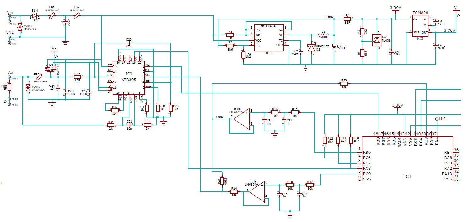
The circuit below has been powered with Vin = 24V and Ax connected to Power supply 0V via a DVM in current measurement mode. Accidentaly the GND connection of the circuit has been left floating which should have been connected to Power supply 0V. On power up DVM showm around 41.5mA flowing through Ax and consequently the IC has been damaged. Could any explain the failure mode of the IC.

  • HI Vithy,

    Can you please clarify what the voltage supplies V+ and V- are?  V- appears to be labeled -3.3V, however the V- supply needs to be in the range of -5V to -20V, where V- supply should be at least -5V.  Are you referring to "Vin" as V+ (pin 15) supply or as the signal Vin (pin3)?  

    Is the Exposed Thermal Pad connected to GND?

    What voltage supply is used to power the LMV324 ?

    If any of the inputs pins of the device sees a voltage exceeding the (V+) supply by +0.5V or see a voltage below the negative supply (V-) -0.5V, the device may get damaged.  Also the current through any input pin can not exceed +/-25mA during any fault condition.

    Thank you and Regards,

    Luis

  • Hi Luis,

    V+(pin 15) would have seen 24V(Vin) - a diode drop of D1. V- would not have been at -3.3V becuse the GND input of the ciruit was floating. Exposed thermal pad was connected to V- and would have been floating as well.

    LM324 will be powered normally by the 3.3V, but in this case would not have seen any power at all as the GND input was floating.

    DRV (pin 13) was connected to power supply 0V via R35(15R) and DVM in series set in curren mode measurment.

    I have checked the device data sheet (section 8.2.1) prior to designing the circuit which stated "The XTR305 can be used with asymmetric supply voltages; however, the minimum negative supply voltage must be equal to or more negative than −3 V (typically −5 V)."  The device worked within the specification when in normal operation.

    I am trying to understand the failure mode of the device and current flow path when the GND input of the ciruit was floating, which should have been connected to the power supply 0V. Some how  41.5mA current was flowing through the DRV (pin 13) and DVM to power supply 0V when the DGND (pin 16) ,V- (pin11) and exposed pad were floating.

  • Hi Vithy,

    I'm sorry, but your description of failure is totally confusing. Please modify the schematic and sketch in what exactly the connections were during the failure and what was not connected. From where to where was the failure current flowing?

    Kai

  • HI Vithy,

    It is correct that the analog input range and output voltage swing range supported is (V-)+3V minimum, and (V+)- 3V (or 3V from the rail supplies).  It is correct that the device can be powered with assymetrical supplies, however, for clarification, the minimum specified supply to meet the operational performance specification is listed on the electrical characteristics table 6.10, where the device is guaranteed to meet the performance with a minimum supply specified at -5V (page 9, Table 6).  

    If you can comment and/or describe in more detail what is the voltage is seen by the DRV pin, and describe in detail how pins 13, pin 11, and GND pad are left  floating (show connected to GND on the schematic).  Is the device not soldered? Are the positive (V+) and (V-) supplies Grounded when this occurs? 

    Please provide a more detailed description of how every circuit is connected and grounded when the failure occurs on the schematic.

    Thank you and Regards,

    Luis