This thread has been locked.

If you have a related question, please click the "Ask a related question" button in the top right corner. The newly created question will be automatically linked to this question.

OPA551: Power dissipation of Op Amp with an AC input signal, 2kHz square wave, 10Vpp output with 25V offset and 50V single supply

Part Number: OPA551
Other Parts Discussed in Thread: OPA548, OPA547, TINA-TI, OPA549, OPA541

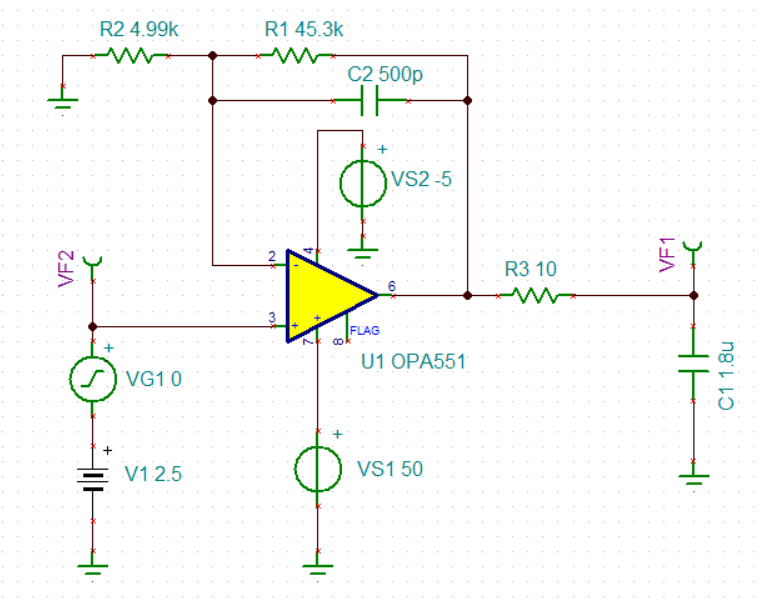
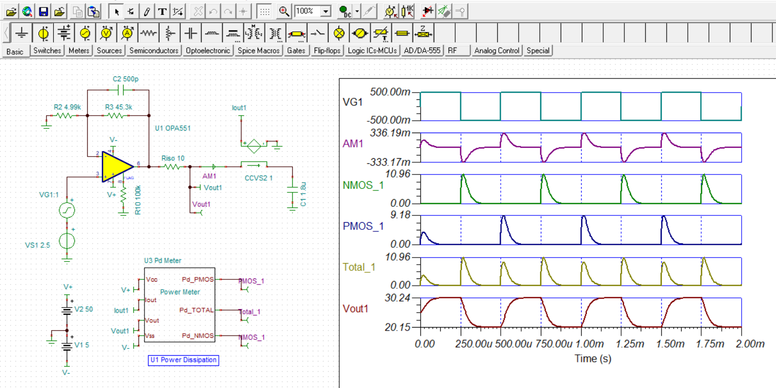
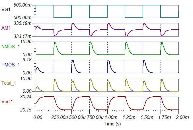
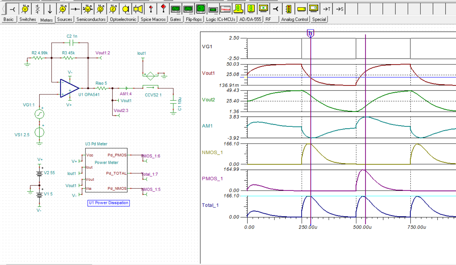
Hi, I am trying to get a power dissipation calculation to find out my thermal dissipation.  I'm using an OPA551 (DDPAK package)  with a 50V single supply.  It's a non inverting amplifier with a gain of 10.  I'm putting in 2.5VDC and 1Vpp, 2kHz square wave signal.  So output is 25V with a 10Vpp swing.  It's going into a 44ohm load.  I have searched for power dissipation formulas and either found them for DC or AC_max that don't include the frequency or voltage swing output that I know are factors based on my testing (for example slowing the signal down cools it down, reducing the output swing cools it down).  Can you help?  Thank you!

  • Hi Elliot,

    you are not only violating the common mode input voltage range but also the maximum output current.

    Or do you use AC coupling at the output? Best you show a schematic of your circuit, please.

    Kai

  • Hi Elliot,

    Once you have addressed the OPA551 operating range issues that Kai identified and the circuit has been corrected to operate within the OPA551 capabilities, I can run a power dissipation simulation. We will need the circuit schematic and operating conditions to get an accurate simulation.

    Regards, Thomas

    Precision Amplifiers Applications Engineering

  • Hi Kai,

    Thank you for pointing out the common mode input voltage to me, I over looked that.  I added a -5V supply to the negative rail and that should fix the issue.

    I am not AC coupling the output.  And I don't actually have a 44 ohm load, it's a 1.8uF cap, I used the 44 ohm load, because that's the capacitive reactance at 2kHz. 

    I am pretty sure I am using the maximum current but I wanted to find out how badly that is going over spec.  That's why I wanted to figure out how to correctly do a power estimation with these parameters and then how much I would have to back off to bring it within spec. 

    I've attached the schematic for you.

    Thanks,

    Elliot

  • Hi Thomas, I did reply not sure if the schematic made it through or not?  Please let me know.  I was hoping I could learn how to do the power dissipation that why when I change the parameters I can run it again.  I've attached the schematic again.  Thanks, Elliot

  • Hi Elliot,

    I ran a quick TINA power simulation on your OPA551 circuit. You can see the results shown below. It looks like the peak dissipation will hit a maximum of about around 10 Watts. The power pulses would need to be averaged to obtain the average power dissipation. See the TINA transient simulation traces labeled PMOS_1, NMOS_1 and Total_1. The OPA551 isn't a MOS power op amp I just borrowed the power dissipation block from another power amp that is CMOS.

    Looking at the OPA551 SOA curves it looks like the power dissipation is too high with this load condition. The OPA547 or OPA548 would be able to handle the power levels you are considering.

    Regards, Thomas

    Precision Amplifiers Applications Engineering

    OPA551_CLoad_PwrDis_01.TSC

  • Hi Thomas,

    Thank you so much, this is great.  I will have to look at it in a little more detail before I reply.  I have been looking at the OPA548 as well, it has a better common mode input range and can drive way more current.  I really appreciate it and will get back to you shortly.

    Thanks,

    Elliot

  • Hi Thomas,

    this is a very nice simulation! I'm amazed :-)

    Is the "PD Meter" part of the free TINA-TI?

    Kai

  • Hi Elliot,

    Glad to assist you with your power op amp application. The OPA548 is a real workhorse and should have no problems meeting your application's power needs. Do let me know if you have any questions about applying it!

    Regards, Thomas

    Precision Amplifiers Applications Engineering

  • Hi Kai,

    The PD Meter is not part of the TINA-TI pull downs, but as you can see it runs in TINA-TI. All you have to do is copy and paste it into your particular simulation circuit when you want to apply the function.

    Full credit for the PD Meter creation goes to our buddy Tim, who has moved on from our TI Precision Amplifiers Applications Engineering team. Nonetheless, his brilliant little tool remains here for us to apply.

    Best Regards, Thomas

    Precision Amplifiers Applications Engineering

  • Thank you Thomas and Kai, this resolved my issue, I am interested in learning more about the PD Meter as well, but can close the issue for now.

    Thank you so much. 

    Elliot

  • Can you expand on how you implemented the CCVS2 and the Pd meter?  That was really insightful. 

    I will use it going forward but wanted to make sure I'm using it properly to obtain accurate results. 

    Thanks,

    Elliot

  • Hi Thomas,

    thank you very much :-)

    Kai

  • Hi Elliot,

    As I mentioned one of my coworkers developed the TINA-TI Pd power meter and it was certainly something that took him some time to accomplish. Since I wasn't involved in its development I don't know the ideas and thinking that went into its creation. In order to understand what role CCVS2 plays in the operation I would have to recreate the entire PD model and then go and learn all of the internal functions. Although that would be interesting, I unfortunately don't have the time to embark on such a project right now.

    Regards, Thomas

    Precision Amplifiers Applications Engineering

  • Hi Thomas, 

    Thanks for the reply.  I understand it is a major undertaking and the reason I was asking is because I would like to design other similar circuits (tweaking different values and trying other op amps) and I wanted to understand the theory behind how to calculate the power with a capacitive load and given parameters.  That way I could work it out, pick the correct device, and then verify it in the simulation and that would give me some confidence in the design. 

    For example now I want to drive a larger voltage into a larger capacitive load.  Most of the analysis for calculating AC power dissipation I've seen will say take the (2*Vs^2)/(3.14^2*RL) which is worst case and will give me 64W for a 50V supply and 8ohm load.  And I know that if I slow the signal down or reduce the input voltage I'm not always going to be dissipating that much power.   

    TI has an excellent presentation on Power and Temperature that is really good https://training.ti.com/system/files/docs/1160%20-%20Power%20and%20Temperature%20-%20slides.pdf but doesn't help me with the capacitive load.  Also I like the application http://www.ti.com/lit/an/sboa022/sboa022.pdf?ts=1591311579503 that describes how to use the Safe Operating Area, but again it tells me for reactive loads use the worst case power dissipation.    Do you know of any other presentations/application notes that have an explanation for large capacitive loads and calculating power? 

    I've tested the OPA548 with a 50V supply and a 10uF capacitive load and the device goes into thermal shutdown around 25Vpp output, and am looking for another device that can give me more output voltage, after I've done some preliminary analysis and identified the requirements.  I'm now looking at the OPA549 and the OPA541 and dropped these into the simulation you provided to me and got unusual results, maybe foldback is occurring, I'm not sure. 

    PART II of my question :-)

    from the simulation you helped me with originally we have an output shown below. 

    To calculate power dissipation, would I take the Vrms*Irms or Pd = 0.707(10.96)*.707(0.333) = 1.82W?

    Thank you so much for your support,

    Elliot

    Elliot

  • image shown below in case it didn't show up in the first message


  • Hi Elliot,

    I think it would be the best, if we could discuss a concrete circuit. Therefore we would need a schematic from you or, even better, a TINA-TI simulation file.

    Kai

  • Hello Elliot,

    The e2e system started crashing my response as I was preparing one for you. I snipped an image of what I was typing before I lost everything. I apologize for the snip-it appearance of my response.

    Regards, Thomas

    Precision Amplifiers Applications Engineering

  • Hi, I've attached two files one for the OPA548, I guess if the part didn't go into thermal shutdown it would work.

    Next is the OPA541, I'm still not sure how much power it's taking.  From some of my calculations I'm expecting 43W.  But this sim tells me it's much larger.  

    I guess the voltage being returned by the capacitive load is doubling the source voltage at the transistors.  

    Thanks,

    Elliot

    OPA548_CLoad_PwrDis_01.TSCOPA541_CLoad_PwrDis_01.TSC

  • Hi Elliot,

    When I examine the OPA541 circuit TINA power simulations it shows that the power maximums occur under conditions you might expect, peak current and maximum voltage across the op amp output transistor that is providing the current. You can see some lines I added to the TINA graphs where the output voltage and peak current result in the peak power dissipation in each output transistor. Vout1 is the voltage directly at the OPA541 output and AM1 is the current it is delivering.

    The peak power is very high, but it looks as though the average of the Total_1 trace is probably about half the peak. The OPA541 may be able to handle the average power without going into thermal shutdown if the thermal requirements are properly addressed. Applications like this require very good thermal management.

    Regards, Thomas

    Precision Amplifiers Applications Engineering

    OPA541_CLoad_PwrDis_02.TSC