Other Parts Discussed in Thread: OPA2810, OPA2810DGKEVM
The datasheet states:
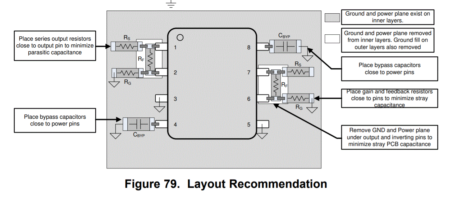
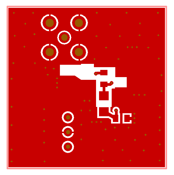
Minimize parasitic capacitance to any AC ground for all of the signal I/O pins. Parasitic capacitance on the
output and inverting input pins can cause instability—on the noninverting input, it can react with the source
impedance to cause unintentional bandlimiting. To reduce unwanted capacitance, a window around the
signal I/O pins should be opened in all of the ground and power planes around those pins. Otherwise, ground
and power planes should be unbroken elsewhere on the board.
For the power planes around the input signal, can anyone show me the design of the layout to acheive:
"To reduce unwanted capacitance, a window around the signal I/O pins should be opened in all of the ground and power planes around those pins. "