This thread has been locked.

If you have a related question, please click the "Ask a related question" button in the top right corner. The newly created question will be automatically linked to this question.

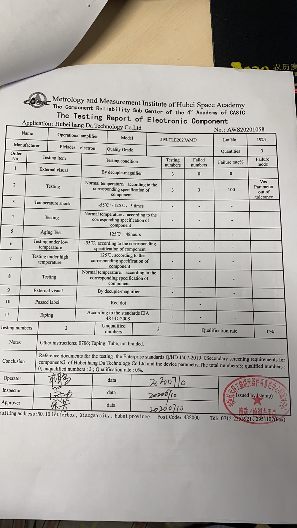
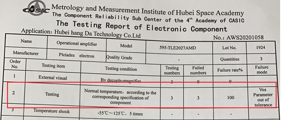
Vos out of tolerance was measured by TLE2027AMD at room temperature.

Other Parts Discussed in Thread: TLE2027

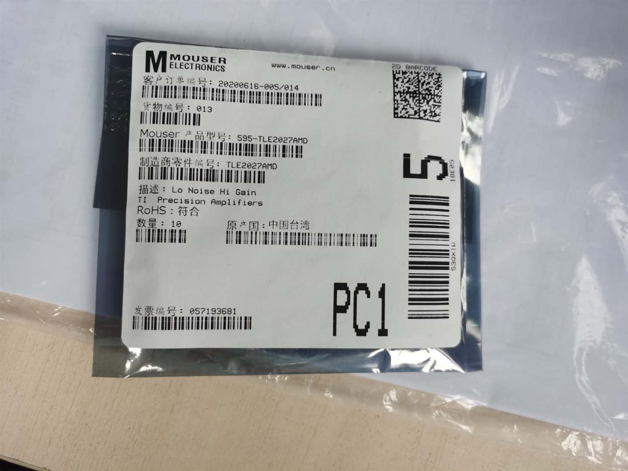
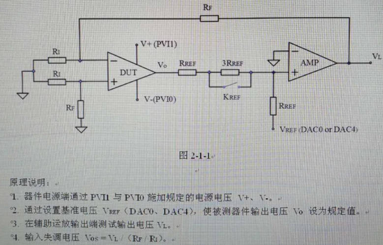
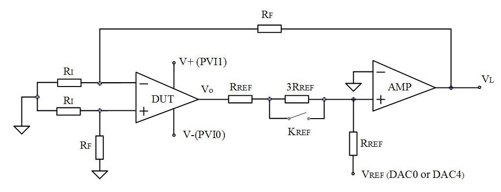
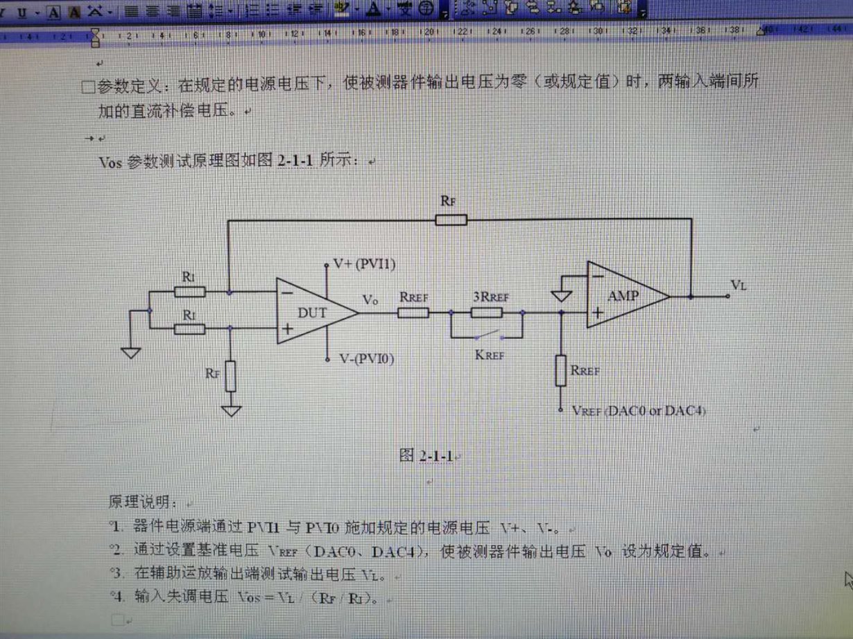
Hello, the amplifier tle2027amd purchased on mouser is out of Vos during the initial test at room temperature. Is this a product quality problem?And it was detected according to the principle in the picture.
  • Hello User , welcome to the e2e forums.

    Please provide the test setup conditions and Vos results.

  • Hi ,

    As Ron pointed out, please provide all the details about the test. 

    Here are the information what we'd like to have:

    1. DUT = TLE2027AMD, I assume

    2. What is AMP model number at the second stage? 

    3. Please provide us with R1, Rref, PV11. PV10, Rf and Vref values. 

    4. What are expected V_L and Vos (What is passing criteria)?  Is last stage a buffer, comparator (Op Amp) or gain stage per your intention in the schematic? 

    5. How are Offset N1 and N2 connected during test? Both pins should be disconnected per recommendation on p.31 in the datasheet,  if it is not used.

    I'd need to above parameters in order to answer your questions. Per the "failure" report, I assumed that Vos is tested at room temperature. 

    Best,

    Raymond

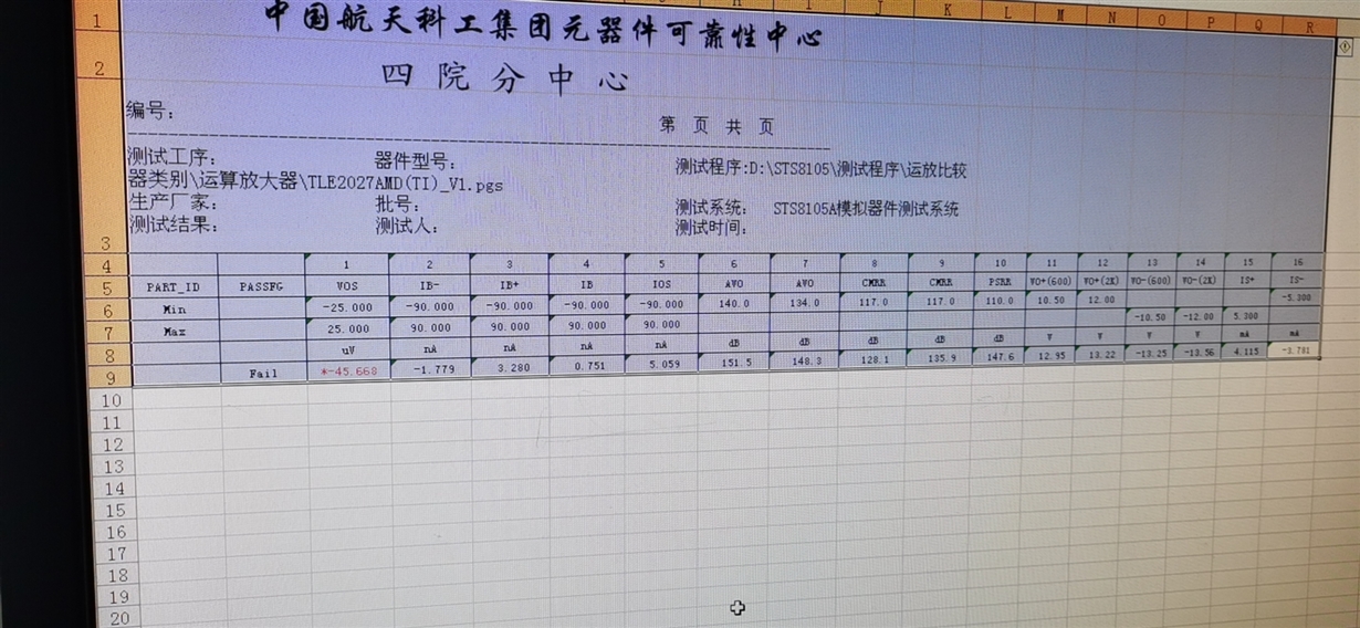
  • Hello, please refer to the following test data, thank you

  • Hello, please refer to the following test data, thank you

  • Hi ,

    Vos is defined as differential input voltage that would have to be applied to force the op amps output to 0V. And Vos is modeled as an internal DC source connected to the non-invert input of an op amp or V+. Changing power supply voltage and common mode voltage will affect the input offset voltage. 

    BTW, in order for the simulation result to match the offset specification in the datasheet, the same test conditions must be applied to the amplifiers. 

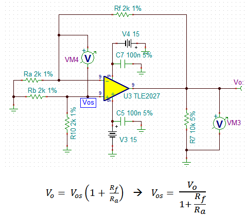
    From the definition, the Vos transfer function should be:

    I do not have the actual R values in your test circuit, so I make up ones.  

    请告知您的测试电路中的实际电阻值.

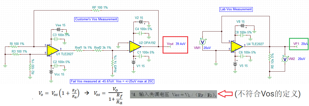
    If Vos = -45.67uV from the test stand, the Vos per transfer function above should be -45.67uV/2 = -22.84 uV (assuming the circuit gain =1).

    The circuit on the right below is how TI is used to measure Vos in the lab. The simulation model is based on TLE2027C. You have TLE2027AMD part, which it should have better Vos ratings than TLE2027C part. 

    Enclosed is the simulation found above. If you have any questions, please let us know. 

    /cfs-file/__key/communityserver-discussions-components-files/14/TLE2027-Vos-Measurement-08132020A.TSC

    Best,

    Raymond

  • Hello TI customer,

    I recognize your test circuit to be the "two op-amp servo test loop".  As Raymond mentioned, it is critical that the test conditions such as the power supply match the Vos conditions of the datasheet, else PSRR for instance must be accounted for.

    But possibly a bigger contributor is the value of your input resistor.  Note that the Vos spec is given with Rs=50 ohms.  If you were to put a larger resistor, you'll be subject to additional errors from Ib/Ios.  So please do provide all of the resistor values and voltage levels in the test circuit.

    It should also be noted that the two op-amp servo loop is a composite amplifier in itself, sometimes requiring additional precautions to maintain stability.  Rather than just placing a DC meter on the output of the servo loop, you should also place an oscilloscope (and do a simulation to assure your composite amplifier has sufficient phase margin). 

    Thanks,

    Scott

  • Hi,

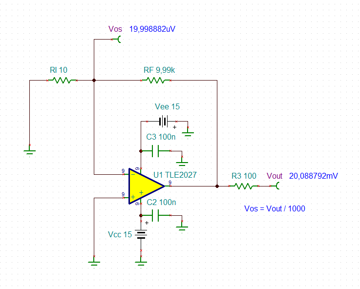
    for checking only the input offset voltage Vos of TLE2027, I would use this circuit:

    tle2027_offset.TSC

    As Scott already mentioned, higher feedback resistances are highly counterproductive when checking only the input offset voltage, because of the unwanted voltage drop of input bias current. Maximum input bias current of 150nA results in a voltage drop of 150nA x 2kOhm = 300µV, which is double the maximum input offset voltage of TLE2027! Across 10R only 150nA x 10Ohm = 1.5µV will develop, which is negligible.

    Kai

  • Hello:

    About your question of double operation TLE2027AMD test, now reply you as below.

    1. Selection of components in test lines

    Figure 1 Vos Principle of parameter testing

    1)DUT= device under test, i.e. TLE2027AMD;

    2)AMP components selected for testing equipment, involving the manufacturer's trade secrets inconvenient disclosure;

    3)R1=100Ω;PVI1=15 V( positive), PVI0Ω;PVI1=-15 V( negative); VrefΩ;PVI1=0 V;RFΩ;PVI1=999.9

    4)VL is the result of measurement;

    5)The N1,N2 pin of the 5) device is suspended during test and no signal is connected.

    1. Questions on test methods

    This test method is the test method of operational amplifier stipulated in the national standard of the people's Republic of China. Our center has used this method to test nearly 100 batches of similar operational amplifiers, such as OP07AZ produced by TI Company, tens of thousands of them.

    The loop construction method of reply in the mail has not appeared in the TLE2027AMD device data sheet provided by TI company's official website.

    2. On RS issues

    RS=50Ω. given in Vos test conditions When the actual test is 100Ω(that is, R1), the difference between 50Ω resistance and 100Ω resistance in the circuit is very small, which will not affect the test results of the device.

    Hope to get your reply soon.

  • Hello, in your reply "3)R1=100Ω;PVI1=15 V( positive), PVI0Ω;PVI1=-15 V( negative); VrefΩ;PVI1=0 V;RFΩ;PVI1=999.9" the value of RF did not show.  I also don't understand for instance PVI1=0V and PVI1=999.9.  Can you maybe label the image itself with all relevant voltages and resistor values?

    Regarding the difference of 50ohms and 100ohms Rs, I would not call it negligible.  At 25C, the 90nA max Ios can contribute up to 9uV.

    Are you seeing one unit testing too high?  Out of how many?        

  • Hi Scott,

    The customer tested 3 parts, and failed 3 parts. 

    Hi ,

    Thanks for providing us with the test parameters.

    Although some of test parameters are still unknown, it is good enough to derive the answer per  your questions. 

    Your transfer function in #4 (see the image below) is missing (1 + Rf/R1). The circuit has Gain =1 in TI's Lab Vos Measurement. The circuit has gain=2 in your ATE circuit. That is part of the reasons that Vos in ATE circuit is measured twice as much as the Lab Vos Measurement. 

    Our center has used this method to test nearly 100 batches of similar operational amplifiers, such as OP07AZ produced by TI Company, tens of thousands of them.

    If Op Amp measured Vos < (Vos_max)/2 in the datasheet, it will pass the above ATE screening criteria, where Vos = VL(Rf/R1). If measured Vos > (Vos_max)/2 in the datasheet, then it will fail the ATE screening with #4 transfer functions. 

    If your screening Pass/Fail criteria is used against the op amp's datasheet, it is recommended that the ATE has to match the test conditions shown in the datasheet.  Otherwise, it is difficult to make apple to apple performance comparisons. 

    Best,

    Raymond

  • Hi ,

    We have not heard from you for about one week. Please let us know how we should help you to resolve the ATE issues. Please let us know.

    Best,

    Raymond