A related question is a question created from another question. When the related question is created, it will be automatically linked to the original question.
If you have a related question, please click the "Ask a related question" button in the top right corner. The newly created question will be automatically linked to this question.
I don't know who designed this circuit so all we can provide is some general information based on a study of the design.
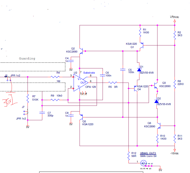
The additional components added to the basic OPA129 buffer amplifier (G = +1 V/V) configuration are there to increase the output voltage swing range beyond the levels that can be achieved by the op amp alone (~+/-13 V). Q3 and Q4 are emitter follower amplifiers and monitor the OPA129 output voltage as the level swings in response to the input level. D1, Q1 and D2, Q6 establish the current through Q4 and Q3, respectively. Q1 drives Q2, and Q6 drives Q5, both of which are emitter followers each connected to the OPA128 V+ and V- pins. They establish the supply voltage levels the OPA128 will operate at as the output voltage swings over the positive and negative voltage range. The purpose of these positive and negative follower circuits is to move the OPA128 V+ and V- supply pins in unison with the output voltage in a manner such that the maximum supply rating of the OPA129 is never exceeded (ABS max 36 V, V+ to V-).
In this circuit you show +36 V being applied to the OPA129 non-inverting input which would appear at the output as well. Following the upper loop from the OPA129 output back to its V+ pin the voltage developed rises/drops across Q4 VB-E, VD1 and Q2 VB-E sets V+ = +36 V + 0.75 V + 6.8 V - 0.75 V = +42.8 V. In a like manner, the output to V- loop is Q3 VB-E, VD2 and Q5 VB-E, V- = +36 V - 0.75 V - 6.8 V + 0.75 V = +29.2 V. If we take the difference in the V+ and V- voltages (+42.8 - +29.2 V), +13.6 V is applied across the OPA129 supply pins. That is within the the specified supply range of +/-5 V (10 V) to +/-18 V (36 V). So it appears the OPA128 V+ to V- supply voltage is set by 2x the D1 or D2 Zener voltage.
As the output moves over a wide voltage range the OPA128 supply voltages move in unison with it maintaining a constant and safe voltage across the supply pins.
Before posting to e2e I tried to understand this circuit. In google search, I found that they used the concept of Bootstrapping(Please correct me if I am wrong).
But when checked about bootstrapping, what I can see is it is a method to to improve the input impedance of the amplifier.
If you don't mind could you please explain the concept of Bootstrapping and how it is applied here(In the above circuit).
There are different forms of bootstrapping applied in analog circuits; the one you mention that raises the input impedance of an amplifier stage, and the other which raises the supply rail operating voltage of an amplifier. I am not sure where the term "bootstrapping" originated in relation to analog circuits but in some way came about from an old 19th century idiom "Pull yourself up by your bootstraps." I believe the intent of electronic bootstrapping is to enhance the performance of the circuit by some manner using minimal additional resources.
Wikipedia has good explanation of "bootstrapping" in electronic circuits. Rather than me attempting to develop a good explanation, I will refer you to their web page.
The bootstrap circuit allows the supplies to move up and down in unison as the OPA129 output moves in response to the input voltage level. When you apply +36 V to the OPA129 input the positive supply V+ moves us to +42.8 V, the negative supply V- move up to +19.2 V. The output will be at +36 V as well, like the input. Note however, you haven't violated the maximum supply voltage across the OPA129 supply pins because the difference between them is only 13.6 V! That is well below the 36 V maximum.
The reason this is safe is because even though there are voltage levels higher than what the datasheet states, pin-to-pin and relative to each other they are well within the specified voltage limits.
I believe C5 is actually part of the OPA129 power supply bypass capacitor arrangement. If I am not mistaken (and I may be), C5's capacitance connected across the Q2, Q5 bases actually gets multiplied by the current gain of the transistors making appear as a much larger capacitance across the OPA129 power supply pins. Since the voltage across the V+ and V- pins stays relatively constant the capacitor only provides current to the op amp only when one supply pin or the other requires a surge current.
Indeed you can do away with all the additional circuitry and use just one high voltage op amp such as the OPA454, or OPA462. They are JFET input op amps as well, but their input bias current isn't as low as the lower voltage OPA129. Do note as well that TI has discontinued the OPA129 and it best not to design anything that would use and call for the device. We have stopped manufacturing it.