Because of the Thanksgiving holiday in the U.S., TI E2E™ design support forum responses may be delayed from November 25 through December 2. Thank you for your patience.

This thread has been locked.

If you have a related question, please click the "Ask a related question" button in the top right corner. The newly created question will be automatically linked to this question.

TLE2072A: Active attenuator output spikes

Part Number: TLE2072A
Other Parts Discussed in Thread: TLE2071, TLE2072, CD4051B, CD74HC4051

Dear Forum,

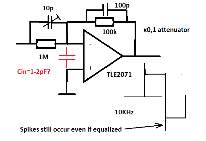
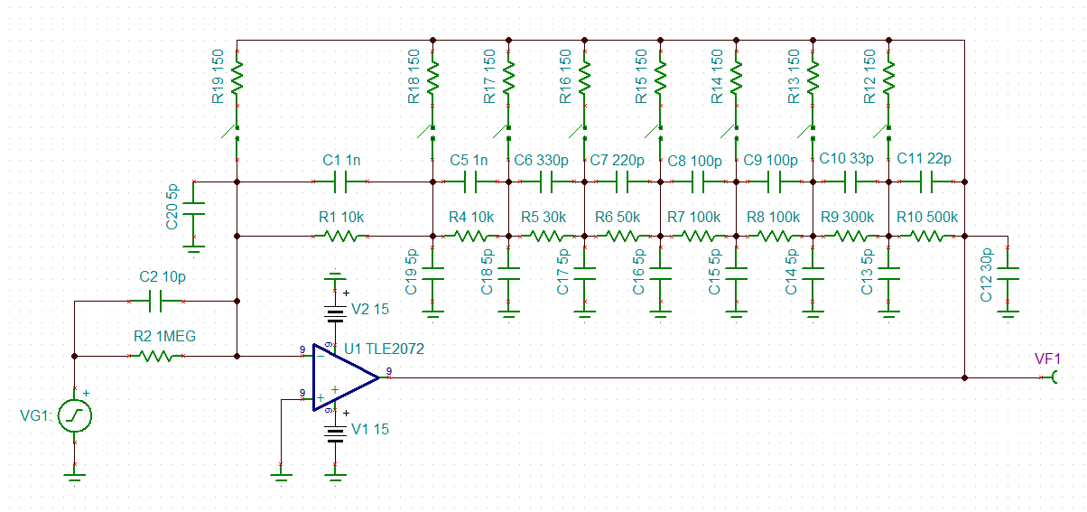
I have bulilt an active attenuator using TLE2072A. This type was choosen thanks for its expectional slew-rate value (>30uV/s) ensuring good signal shape fidelity. Additionally, the circuit has a high input impedance,

thus input/parasitic capacitances had to be compensated. Unfortunately, after compenstaing, large spikes still occur at signal transistions (square wave transition edges). Spikes cannot be trimed out.

I do not understand why the spikes, maybe due to less phase margin (stability issues) and the large capacitances. However, the external compensation shall improve the over stabulity.

Joseph

  • Hi Joseph,

    the edges of input square wave directly punch through the feedback loop to the output of TLE2071 via the 10pF and 100pF cap before the OPAmp is able to readjust the output voltage. This can often be seen in inverting amplifiers. The 10pF cap in parallel to the 1M resistor is counterproductive here.

    Possible remedies are:

    1. Llimiting the slew rate of input signal.

    2. Drastically decreasing the feedback resistances.

    3. Using a passive voltage divider and a voltage follower.

    Kai

  • Hi Kai,

    thank you for the Quick and valuable answer! You have right: at high frequency contents (signal transitions) the capacitors exhibit low impedance overdriving opamp before it could react (final propagation delay inside the amp). It might be analougus to the "speed up capacitor" parallel to base resistor used in the early RTL logic circuits.

    The #3 option is the best solution for me (I cannot decrease input impedance).

    Joseph

  • Hey Joseph, 

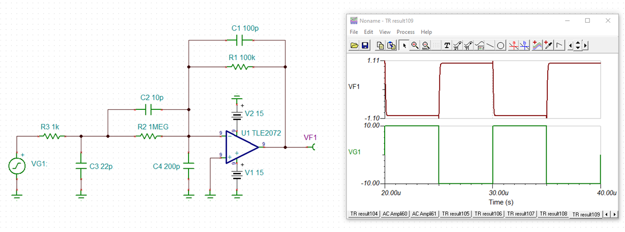
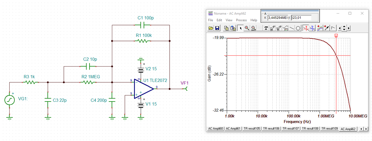
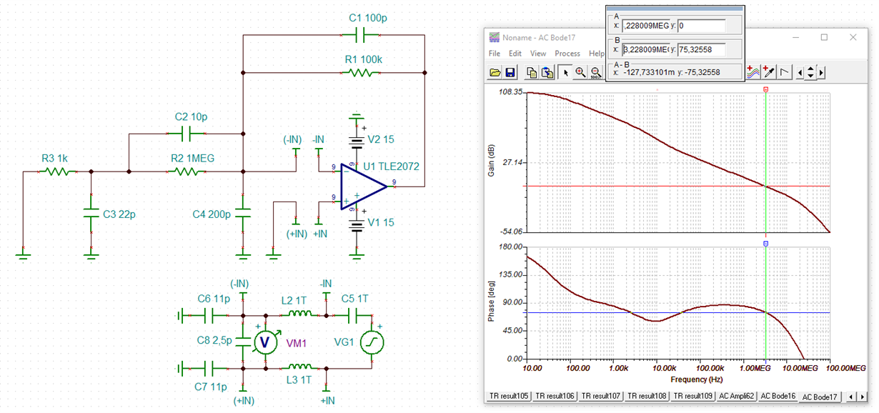
    You did not say how fast your input edges are nor how fast the overall response needs to be, Adding the 200pF to ground on the inverting node as shown here shapes the noise gain from 1.1 at DC to 3 at higher F giving very controlled cutoff at about 4MHz, might try that to see if it cleans up your problem, 

  • Also, the slew rate on the TLE2071 is very asymmetric as shown way back on page 55 - shows up in sim also, there much better (newer) parts to use if you could provide supply voltages and package, 

  • Joseph,

    I suggest a passive divider (IN to ground) and a unity gain buffer. The frequency neutral compensation will work well on the passive input divider. This makes the circuit non-inverting, is this acceptable?

  • Hi Michael,

    thank you for the remark! It sounds interesting, however I do not understand fully. I made a simulation in TINA adding 220pF cap between "-" and GND but the spikes still present. However, the 4MHz bandwidth just OK for me.

    Joseph

  • Hi Ron,

    I wanted the active attenuator because it has a benefit: provides a virtual GND and high voltage (>10V) only across the RIN resistor (source and "-" terminal).

    RF resistor can changed by an analouge MUX.

    Yes, I may turn to passive divider and opto-isolated FET switch/ reed contact. analog MUX IC cannot be used in this case.

    Joseph

  • Hi Joseph,

    the spikes are still present because the current path through the 10pF and 100pF caps still exists :-)

    Only the height of spikes has changed.

    Kai

  • Hi Joseph,

    tell something about your input signal. What is the maximum slew rate of your input signal?

    Kai

  • Hi Kai,

    thanks for the remarks! Input slew rate: AHC Logic signal.

    Joseph

  • So Joseph, is this a sim or bench - if sim, do you perhaps have an unrealistically fast input edge - 

  • Here is the circuit running a 100kHz +/-10V input with 100nsec edges (that is still a 200V/usec slew rate input) - looks fine, 

  • Hi Michael,

    no, it is a real circuit. I try to add a 220pF between "-" and GND. I Will came back on Monday with the result.

    Joseph

  • So are you saying you have not tried that yet? And, again, what is your input signal step size and edge rate - all of this will simulate if we had the necessary data.

  • Hi Joseph,

    74AHC-MOS is producing output rise and fall times of about 1...2ns depending on the capacitive load. So the spikes in the simulation seem to be realistic.

    I would do it this way:

    joseph_tle2072.TSC

    R3 and C3 do not only provide a low pass filter for the fast 74AHC-MOS signal and by this soften the edges, but R3 also limits the inrush current into the series circuit of C1 and C2. Both results in a decrease of spikes.

    And the phase stability analysis shows a very good phase margin:

    joseph_tle2072_1.TSC

    Keep in mind that your planned analog switch (MUX) will change the capacitance seen by the TLE2072 at its inverting input. So you should choose a MUX with acceptably low switch capacitances.

    Kai

  • That looks great Kai, I guess I missed somewhere along the way what was driving this - yes, 2nsec input edges will usually come through an inverting attenuator as pre-shoot. 

  • Hi Kai, thank you for the detailed analysis. The 220pF capacitor did not helped. My source resistance is 600Ohm (series resistor to AHC04 gate output)

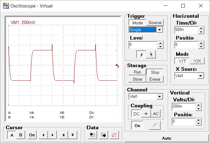
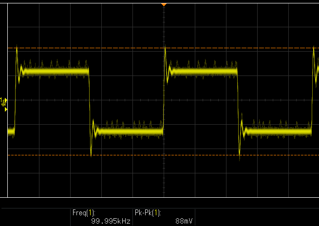
    The AHC04 is only a reference/calibaration signal. I tr to send scope waveform. My TLE is working from +/-5V.

    Can you pls tell me about L1/L3 network? Note, the TLE output is connected to an MSP430 MCU (it generates test signal for AHC04 as well) whose A/D has a bandwidth

    2MHz. Note, prior to A/D, 1/2 TLE2072 configured x (-2) amp + provide 0,75V offset (unipolar A/D range :0..1,5V).

    Joseph

  • Joseph,

    I agree with Kai's addition of the input low pass filter to dull the input edges. In the second circuit, ridiculous value for L2,3 and C5 makes the 'L' a short at DC and open for any practical frequency, AC. C5 is the opposite, it is open at DC and a short for any practical frequency, AC. Consider tem just a tool, to check the stability of the amplifier loop.

  • Hi Joseph,

    this L stuff is explained here:

    Kai

  • Hi Kai, Ron,

    thanks for the suggestion. However, for these a new PCB needed.

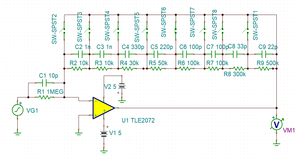
    Meanwhile I found some issue in the circuit: the compenstaing resultant capacitor was not 100pF but much smaller (resistors at the feedback path - analog MUX: 10k,10k,30k,50k etc, and caps parallel to them in order: 1n, 1n, 330p, 220p..), the second cap was 105pF only! Thus, it seems an insuffucient compensation also existed. Maybe accidentaly a wrong value was mounted or the cap is faulted because its shade (color - light grey) and pads shape are the exactly same to 1n type. So I do not think I mixed them.

    Now, the waveform at the out of the inverting compensated amp (input 500mVpp, G=-0,1): Result is much better but smaller spikes still present.

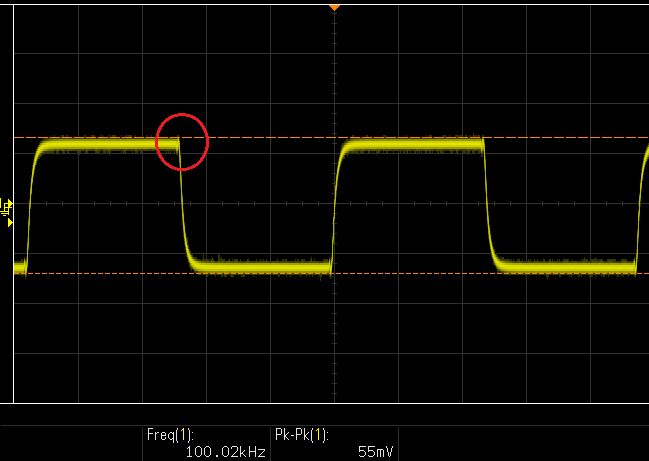
    At the output x2 inverting amp: (resulting a non-inverting waveform):

    After adding 10pF parallel to the feedback resistor: only small amout of overshoot can se seen:

    Joseph

  • Joseph,

    Are the new waveforms acceptable to use the circuit as it is now built?

  • Hi Ron, Kai

    I think so, Thank you vm for the help and your time.

    Joseph

  • Hi Joseph,

    Meanwhile I found some issue in the circuit: the compenstaing resultant capacitor was not 100pF but much smaller (resistors at the feedback path - analog MUX: 10k,10k,30k,50k etc, and caps parallel to them in order: 1n, 1n, 330p, 220p..), the second cap was 105pF only! Thus, it seems an insuffucient compensation also existed. Maybe accidentaly a wrong value was mounted or the cap is faulted because its shade (color - light grey) and pads shape are the exactly same to 1n type. So I do not think I mixed them.

    I haven't fully understood what you said there. Can you please explain? And can you show your latest schematic? Also, which modification resulted in your last scope plot?

    Kai

  • Hi Kai, sorry for late answer, I was not able to watch the forum.

    Here is the schematic.  Switch is CD4051B IC. The C3 was only 105pF. Additionally, after this active attenuator there is an additional G=-1 inverting amp (not G=2 as written previously...it is worse case than G=2) and I add 10pF to Rf (10k) for this amp too (2nd part of the TLE2072). Therefore the spike was also caused en excessive differentiation effect which could not be trimmed out due to too low C3 value.

    However, your explanation on the narrow spikes (amp overdrive effect by the caps and amp internal propagation time), stability issues are very usefeul for me to understand better the nature of inverting amps.

    Other question: could you offer an uncompesated FET/CMOS amplifier with similar paramaters (SR>10V/us, GBW>10MHz). Internally uncompensated amps are quite rare nowadays..

    Joseph

  • Hi Joseph,

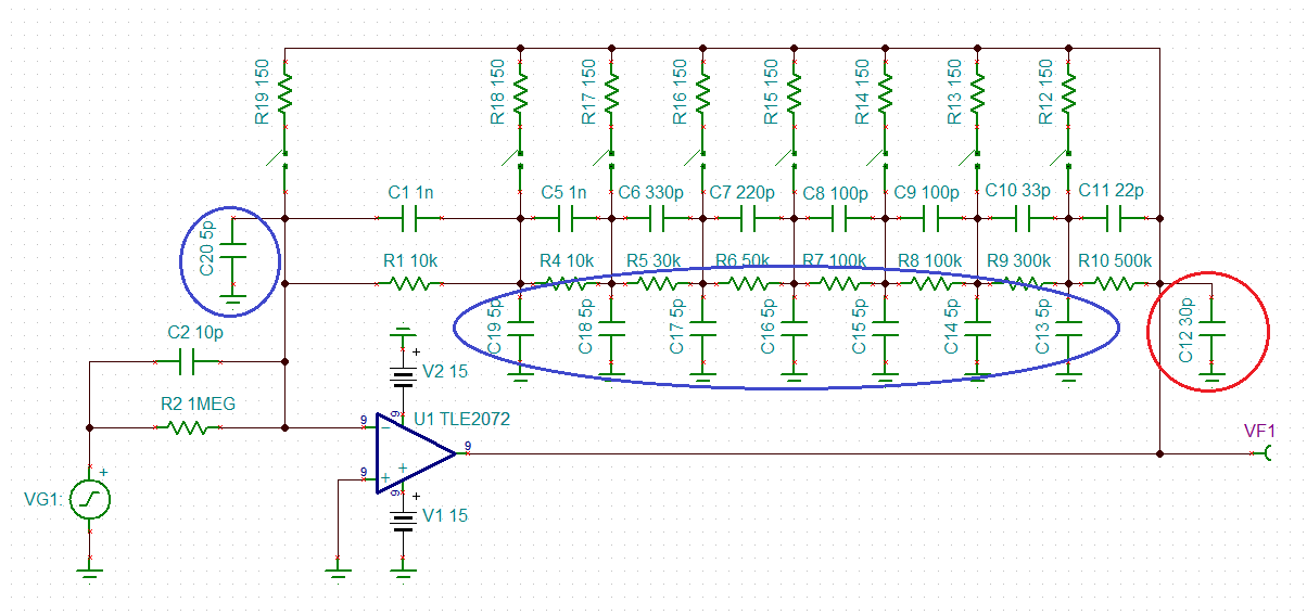
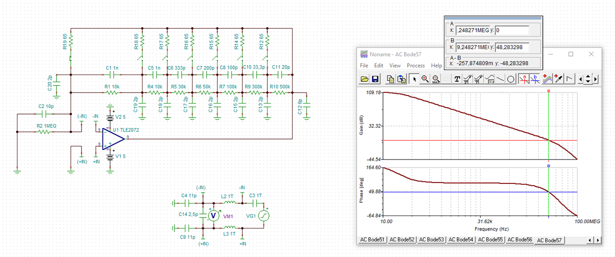
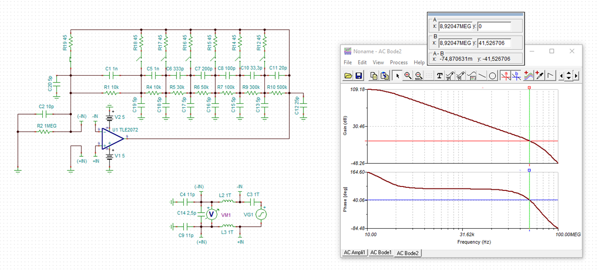
    a more complete schematic including the parasitic elements of multiplexer CD4051 would look like this:

    joseph_tle2072_2.TSC

    Kai

  • Hi Kai,

    thanks for the remark! I considered these elemets: in my physical circuit the MUX common (30pF) is at the amp output not at inverting input.

    Joseph

  • Hi Jospeh,

    like this?

    Kai

  • Hi Kai,

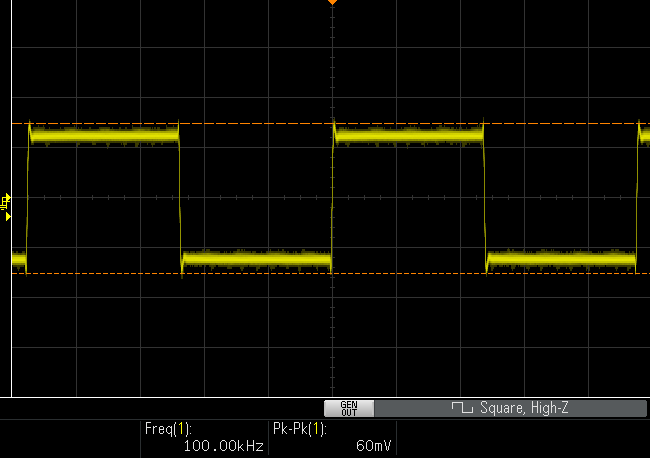
    yes, I show a waveform measured at the U1 output when 5th switch is ON. There are some residual over/undershoot (compensation at optimum by C2 trimmer). May I add a 5..10pF between U1 "-", "OUT"? However, it is seems a ringing and not due to inadequate compated attenuator Network.

    Because the ringings are always considered as source of noise/EMC issues.

    I can response on next week monday.

    Bye

    Joseph

  • Hi Joseph,

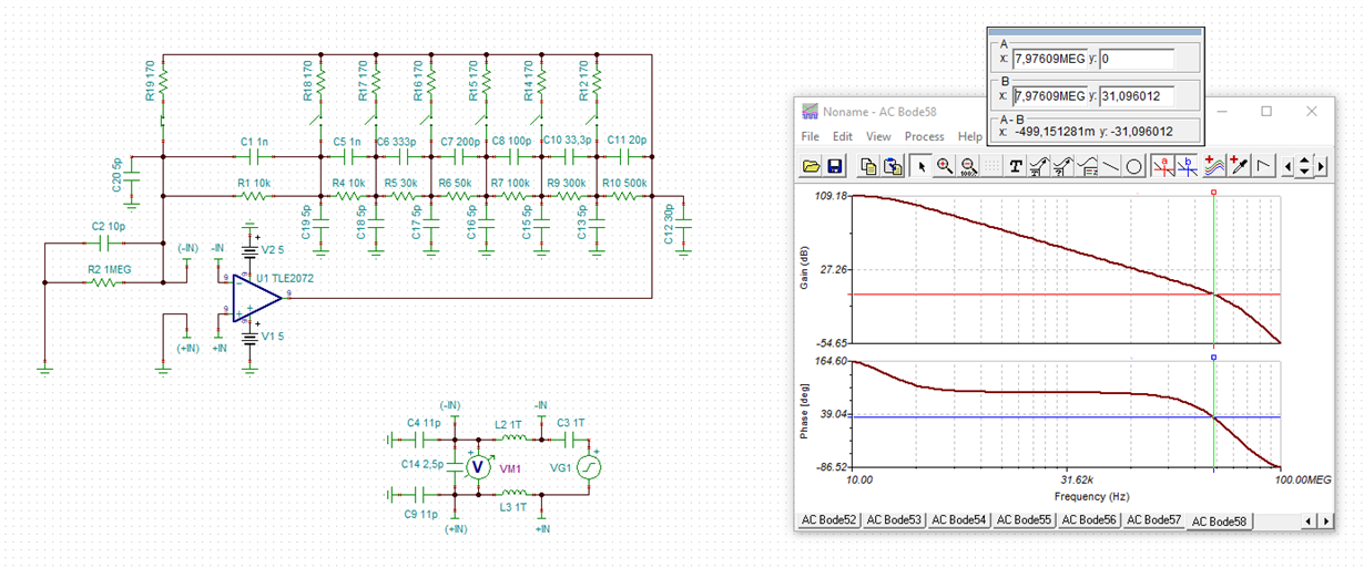
    the parasitic elements of CD4051 ruins the stability of your circuit and results in a phase margin of only 31°:

    Reducing the parasitic elements, for instance by using the MAX4051, improves the phase margin to 48°:

    6835.joseph_tle2072_2.TSC

    Kai

  • Hi Kai,

    thank you for the in-depth investigation and for the TSC file. I have chacked: phase margin highly influenced by the Ron of switches. Unfortunately, momentary I do not have MAX4051A IC to try.

    May 74HC4051 be enough?

    I have learned again something: a good practice how to perform open loop gain measurmeents in TINA: apply very high inductances braking loop by aspect of AC while keeping it closed by Dc point of view (needed to biasing the OPA), additionally, use a very high capacitance coupling AC excitation.

    Joseph

  • Hi Joseph,

    it's true that the lower Ron resistance of CD74HC4051 may imrove the stability a bit:

    But also the parasitic capacitances of multiplexer play a role when it comes to stability here. So I would recommend to use the MAX4051 or a simlar product showing very low parasitic elements.

    Another issue is charge injection. As the CD74HC4051 is much faster than the CD4051, toggling the control signals will result in much more switching noise. Here again the MAX4051 is of benefit.

    Kai 

  • Hi Kai,

    I do not understand fully: why does not a slight overcompensation (products of RfCf>R2C2) improve the phase margin? Equivalently, a lowered  C2  value (which is trimmable)? ->"remained " capacitance in feedback path might act an external compensation to the opamp.

    Or, if Gain<<1, the Cf is not effective? Quite complicated (for me). I think we arrived to the depth of analog theory :). 

    Have a nince week-end! I cannot be reached until Moday (due to limited internet Access..).

    Joseph