This thread has been locked.

If you have a related question, please click the "Ask a related question" button in the top right corner. The newly created question will be automatically linked to this question.

AMC1211-Q1: Unspecified Behaviour of AMC1211-Q1, goes into safestate for small timesteps even with a stable supply

Part Number: AMC1211-Q1

Hello everyone, since the direct support couldnt help any further, they suggested posting here:

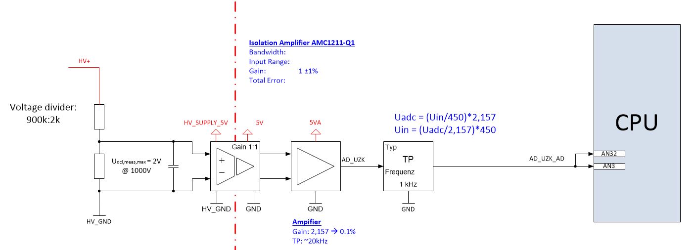
As the title says, we are having some problems with multiple chips of the Type AMC1211-Q1. As intended, the chip is used for an analogue isolated voltage measurement, see the path architecture below.

It is used in a traction inverter with with 820V/660ArmsAC output. with high output currents, the AMC chip does not behave as intended.

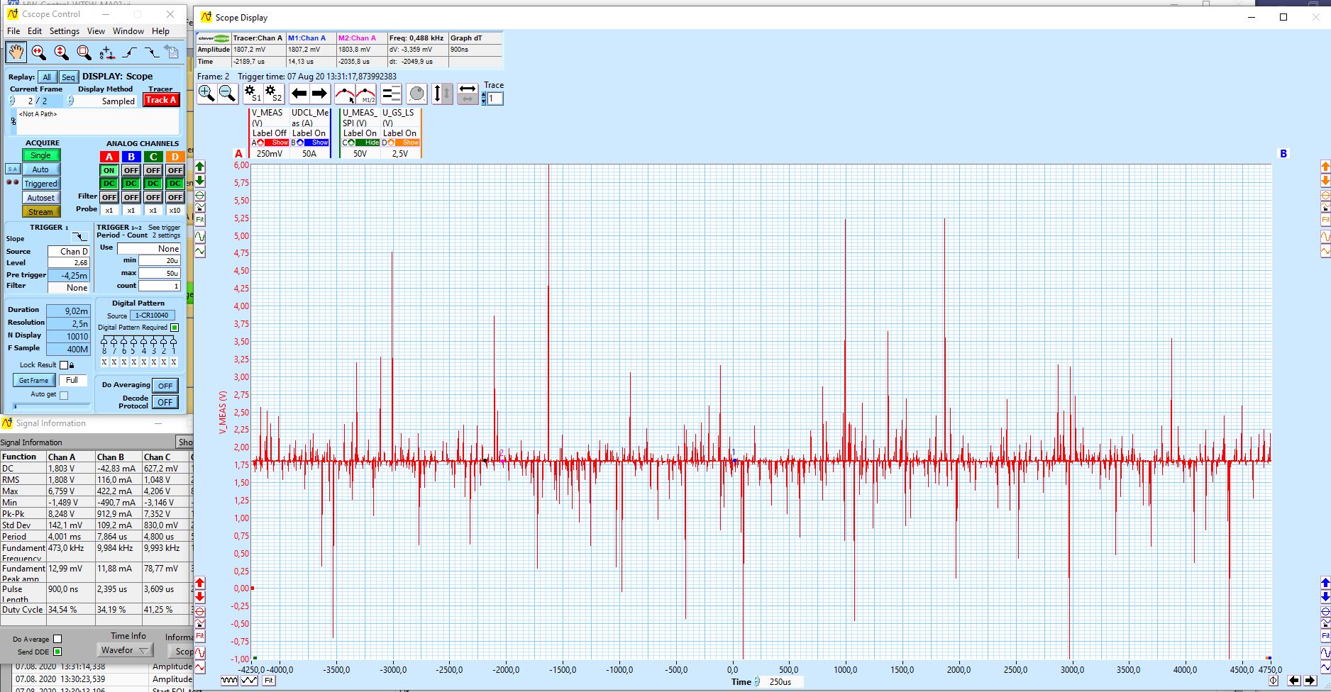
The differential ouput either goes into safestate (-2.5V) or clips positive (2.6V) for some short periods of time. Please see the measurement graph below. In red: 5V Supply of the HV-Side, measured directly on the pin of the AMC, in blue, the differential output. The measurement voltage remains stable, as seen in the second graph in red.

We could verify this behaviour on different DUTs. Any help here?

Thanks alot,

best regards,

Lukas

  • Hi Lukas,

    Can you share your actual schematic instead of a block diagram? I can contact you offline if you do not want to share on the forum. 

    It looks like you have some significant noise in the system. More than likely, you are seeing this behavior from the AMC1211 due to this noise. The absolute maximum rating for VDD1 voltage is 6.5V. From the first picture, I cannot see if the noise reaches this magnitude, but it is getting close to potentially damaging the part. As this noise returns to GND, the device is being put in and out of fail-safe mode, full-scale positive, and common-mode violations may occur as well. 

    What type of filtering do you have on the power supplies and input? We typically reccomend and RC filter with a 1MHz cutoff frequency on the input. For power supplies, bulk capacitance (1-10uF) near the source, with a smaller capacitor (1-10nF) near VDD1. 

    On a system level, what does your grounding look like for the high-side? 

  • Hi Alexander,

    id prefer to share the schematic page directly, not in the forum. As for the measurement peaks, the peaks are significatly influenced by the actual switching noise, since the inverter is SiC based, we do have significant noise in the system (as you guessed).

    It is not possible to measure an "absolute" level somewhere due to those peaks. 

    There is a lot more info to provide, id prefer to do that also privately

    The Ground is referenced to the source of only one lowside module with 0Ohm, both other LS-sources are floating. The GND should therefore be stable versus the DCL-Ground. 

    Best regards,

    Lukas

  • I'll shoot you a note to continue the conversation offline.