This thread has been locked.

If you have a related question, please click the "Ask a related question" button in the top right corner. The newly created question will be automatically linked to this question.

OPA211: The bias current questions

Part Number: OPA211
Other Parts Discussed in Thread: OPA2210, OPA828, OPA320, LMP7721, OPA192

Hi,

I am a hardware engineer. I have some questions about the op amp bias current.

Q1: The bias current is supplied by the external circuit or the internal circuit?

Q2: If the bias current is supplied by the external circuit, for the invert amp circuit:

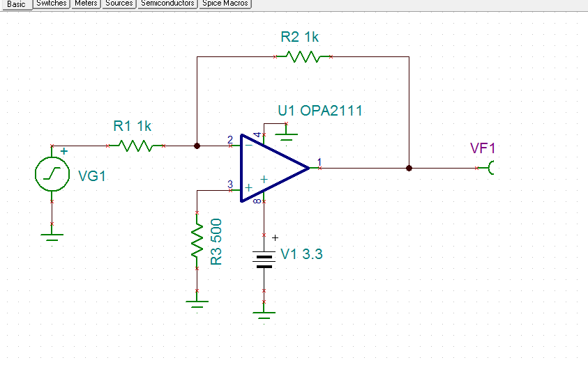
 As below fig, VG1 and VF1 can supply the bias current to the 2 pin?

the 3 pin is connected to GND, who can supply the bias current to the 3 pin?  I do not believe GND can supply the bias current to 3 pin.


                                                                                          FIG1

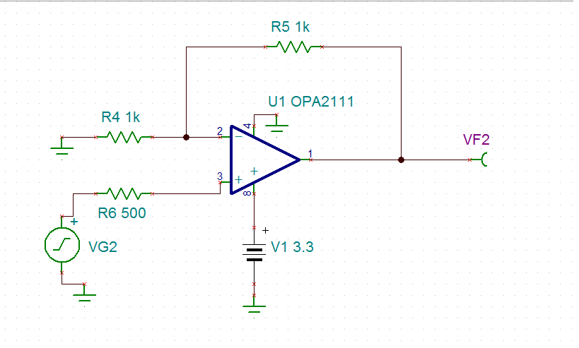
Q3: As below FIG2, For the phase amp circuit, VF2 can supply the bias current to 2pin?

                                                                FIG2

Q4: The output offset voltage is only affected by the  bias current part: For FIG1, Vos= Ibias*(R1//R2)*Gain; For FIG2, Vos= Ibias*(R4//R5)*Gain, Correct?

If it is correct, I want to get why it is the (R1//R2) value and the (R4//R5) value? How to calculate?

Q5: I get use R3(fig1) and R6(fig2) to eliminate the bias current influence, correct?  

If it is correct, why R3=R1//R2 and R6=R4//R5?  How to get and derive the  formula ?

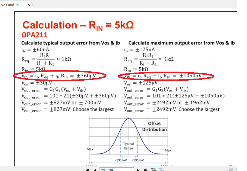
Q6: I watched TI Precision Labs. I have a question as below: The offset voltage for the bias current is: Vib=ib*Req+ib*Rin.  But Vib=ib*Req-ib*Rin is not correct? Why? How to get and derive the Vib formula ?


Q7: How to select the TIA op amp for the bias current? the bias current is less than the input current? Why? If the bias current is higher than the input current, what will happen to this?

  • Hi,

    the input bias current of a BJT input respectively the leakage current of a CMOS or JFET input flows automatically. But you have to assure that this current can flow by providing a current path to signal ground. So the input bias current can flow into or out of signal ground or a supply voltage and into or out of the output of an OPAmp.

    Kai

  • Hi Kai,

    Thanks for your reply.  But I have 7 questions and I think your reply is very simple, And I cannot understand your meaning. 

  • Hi,

    what can you not understand :-)

    Kai

  • Hi,

    I have 7 questions. If you want to help me reply the questions, I hope I can get 7 answers one by one. Not simple reply. 

    I need a detail reply.

    However, I need a TI expert to reply my questions.

  • Hi,

    Can  TI expert help me to explain this?

  • Hello user4674678,

    Q2: If the bias current is supplied by the external circuit, for the invert amp circuit: As below fig, VG1 and VF1 can supply the bias current to the 2 pin? the 3 pin is connected to GND, who can supply the bias current to the 3 pin?  I do not believe GND can supply the bias current to 3 pin.

    I am not sure you realize you are showing an OPA2111 legacy audio op amp in the circuit, but I think you intended instead an OPA211 as in the title of the e2e indicates. Additionally, the OPA211 has a minimum supply of +4.5 V so the +3 V would be too low to power it. Then, if you do use a single supply of the proper level the input common-mode range and output relative swing range to ground would have to be observed.

    Yes, VG1 and VF1 provide paths for the input current to the inverting input. The non-inverting input would have to be set to a voltage level within the rated common-mode voltage (VCM) range of the OPA211, (V–) + 2 to (V+) – 1.4, for VS < ±5 V. Its input current would be provided by this voltage source. If a dual supply were used and the non-inverting input is connected to ground (VCM = 0 V), then indeed ground could source or sink current through the OPA211 input circuit.

    Q3: As below FIG2, For the phase amp circuit, VF2 can supply the bias current to 2pin?

    Noting the issue with the circuit that are not correct and correcting them, the signal source would provide the input bias current for the non-inverting input.

    Q4: The output offset voltage is only affected by the  bias current part: For FIG1, Vos= Ibias*(R1//R2)*Gain; For FIG2, Vos= Ibias*(R4//R5)*Gain, Correct? If it is correct, I want to get why it is the (R1//R2) value and the (R4//R5) value? How to calculate?

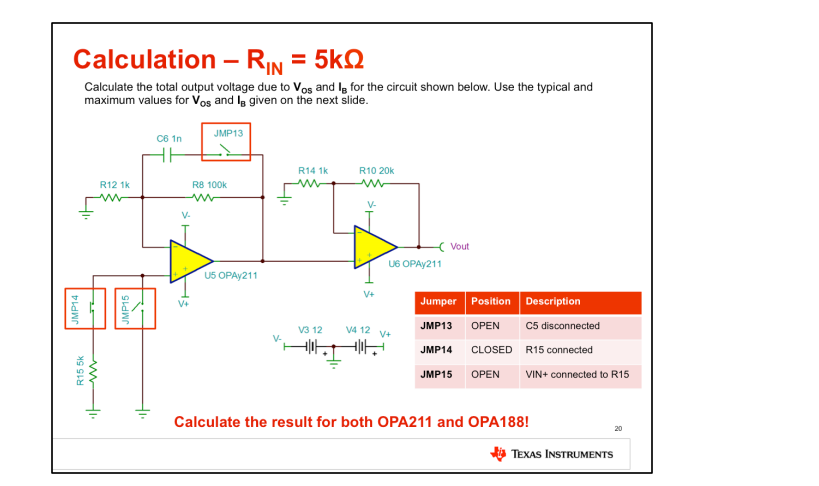
    No, the total output referred voltage offset is the combination of the op amp's input voltage offset, each input bias current flowing through their individual resistive paths, and the gain by which they are multiplied. see:

    https://training.ti.com/zh-tw/system/files/docs/1100%20-%20Vos%20and%20Ib%20-%20exercises-and-solutions_0.pdf

    Q5: I get use R3(fig1) and R6(fig2) to eliminate the bias current influence, correct?  

    The resistor you have added in series with the non-inverting input may be used to reduce the voltage offset introduced by input bias current flowing through the inverting input's equivalent resistance (Ri || Rf) for op amps whose input current flows in the same direction. This is common for bipolar input op amps that don't use any special input bias current cancelation. FET input op amps and bipolar input op amps that use bias current cancelation may have input currents that flow in opposite directions. Adding the series resistor may decrease the offset or increase the offset depending on the magnitude of the two input bias currents. In general we don't suggest adding this resistor in any op amp circuit because input bias current are very low in general. The resistor was often added when op amp inputs were strictly bipolar and their input currents were often in the tens-of-microamps!

     Q6: I watched TI Precision Labs. I have a question as below: The offset voltage for the bias current is: Vib=ib*Req+ib*Rin.  But Vib=ib*Req-ib*Rin is not correct? Why? How to get and derive the Vib formula ?

    The direction of the input bias current (Ib) through each input will affect whether their individual contributions to the output referred offset is the sum or the difference. Have a look at the link I provided. The TI Precision Labs - Op amps, is really quite complete on the subject.

    Q7: How to select the TIA op amp for the bias current? the bias current is less than the input current? Why? If the bias current is higher than the input current, what will happen to this?
    Op amps used for transimedance amplifiers are usually selected such that their input bias current is many decades less than the current produces by the current source, which is typically photodiode. Doing so helps prevent the op amp from loading down the current source and introducing error. This is why JFET and now CMOS FET input op amps are most often used for the application. The newer super-beta bipolar input op amps such as the OPA2210 have very low input bias current, but not quite as low as what can be had with the FET input op amps. They certainly will work if the current source produces an output current much higher than their bias current.

    Regards, Thomas

    Precision Amplifiers Applications Engineering

  • Hello there

    Regarding your question for TIA's, Thomas is correct in that it's usually JFET's or CMOS inputs that make a good choice. However, the selection can be rather broad even within these 2 process technologies. One of the lowest Ib op amps in the industry is the LMP7721, this one great if the application requires a wide temperature span. If the temperature is well contained, then the OPA320 is good choice given its low Ib and fast settling. Now, these are low voltage op amps and if a higher supply (up to 36V) is needed, a JFET like the OPA828 would be suitable as would be the OPA192 (CMOS).