This thread has been locked.

If you have a related question, please click the "Ask a related question" button in the top right corner. The newly created question will be automatically linked to this question.

ALM2402F-Q1: gain error

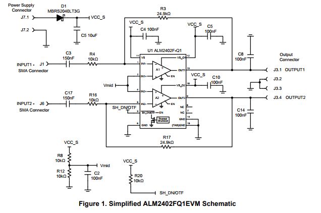
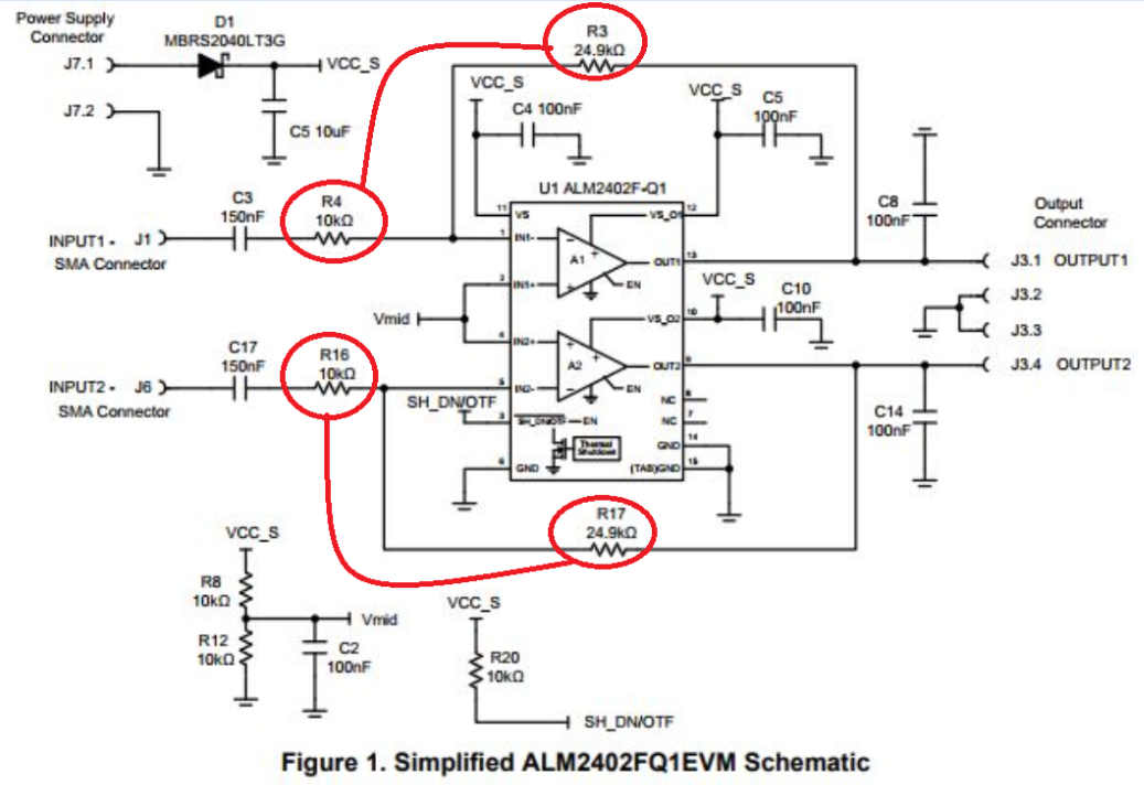
Part Number: ALM2402F-Q1

Hii 

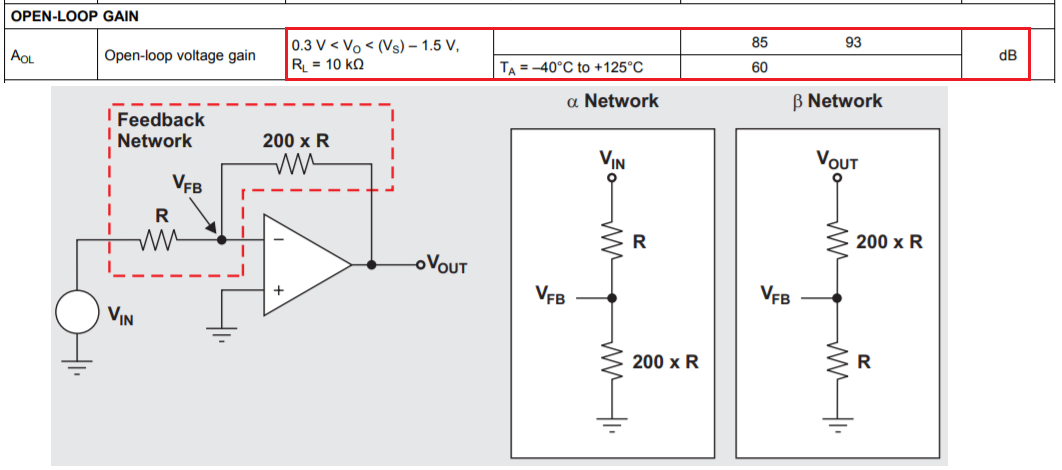
I was using th ALM2402 IC for resolver excitation circuit. I was calculating the error budget calculation. Can i know the gain error of the IC.

Regards

Bharath Gilla

  • Hi  Bharath,

    Would you be able to share the resolver schematic with us? I also would like to know that application's excitation frequency and excitation amplitude for the resolver. Without the schematic or amplifier gains, I can only provide you with the datasheet specification. 

    Enclose is the ALM2402F-Q1 EVM application note, you may find it helpful. 

    https://www.ti.com/lit/ug/sbou227/sbou227.pdf?ts=1598293253960&ref_url=https%253A%252F%252Fwww.ti.com%252Ftool%252FALM2402FQ1EVM

    BTW, the dominated errors in an actual resolver are not from excitation driving amplifier, as stated in red box. The dominated error sources are from the rotary transformer couplings and magnetic behaviors of a rotary transformer in an operation. 

    Best,

    Raymond

  • Hii Raymond

    We are using the AD2S1210 IC for RDC and the excitation frequency is 10khz. with resolver excitation voltage is 7Vrms(across output1 and Output2). Input to ALM2402 (INPUT1 & INPUT2) is peak to peak 2.5V offset and 3.6Vpk-pk sine wave.

    Regards

    Bharath Gilla

  • Hi Bharath,

    Question:

    I was calculating the error budget calculation. Can i know the gain error of the IC.

    Before I attempt to do the calculation, I have a couple more questions. What are your resistor tolerances in the feedback loop? I want to make sure that the DC gain error analysis in Figure 1 is what you are looking for, since the question is not very clear (We are talking about IC or the resolver circuit in Figure 1 in ALM2402F-Q1 circuit). 

    From ALM2402F-Q1 datasheet, we have the Aol gain range shown in the image below. 


    If you are talking about DC gain error in the entire operating temperature range, Aol = 60dB will be worst case. With the following equations, we can calculate the DC gain errors in the worst case from -40C to +125C (using Figure 1 EVM driving circuit). 

    From Equation 21 & 22 , DC gain error for a single Op Amp drive can be calculated for the worst case over the operating temperature. (-40C to +125C). 

    Please let me know if the DC gain error calculation in Figure 1 is what you are seeking. 

     Best,

    Raymond


  • Hii Raymond

    Sorry for delay in response, i was struck in between other works. my resistance tol is 1% and cap tol is 5% and R3, R17 value is 27k and R4,R16 value is 10k  C3 and C17 150nF. Presently i was  trying to calculate the worst case phase shift and gain error from input to output i.e ( across INPUT-1 and INPUT 2) to (across output 1 to Output2). also what will be the effect of gain error and phase shift w.r.t to Vmid as below.

    Please let me know how to calculate the worst case gain error and phase shift

  • Hi Bharath,

    From the previous reply, I included on the information about the absolute gain error in ALM2402 IC, which I believe that this is what you are asking for (Can i know the gain error of the IC).

    With the latest reply, what will be the effect of gain error and phase shift w.r.t to Vmid, I think that you are more interested in the Resolver's  system gain errors and phase shift in ALM2402F-Q1 resolver application. Vmid is dc bias point of the op amps input. Phase shift w.r.t. to Vmid does not have issues at the op amp's input side. I think that you may be thinking about the phase shifts of the sine and cosine at the receiver side. 

    The excitation frequency per the application note is 10kHz,(same input with opposite phase), I recalled. Let us assume that it +/-Xppm off from the nominal input of 10kHz, where both half sinewave should have approx the same amplitude with exact opposite shape in phase. The differences of the output is still a sine wave, otherwise, you will not get the sinewave at the output. 

    Before I am answering your questions, I need to know if the excitation coil is directly coupled to the J3.1 and J3.4 as shown in figure 1 or the resolver driving circuit is AC coupled to the excitation coil.  

    If the excitation coil is directly coupled in the resolver applications, it is not an absolute gain error that matters but rather a mismatch between the gains of two signal paths.  For this reason, it is the matching of R3/R4 to R17/R16 that is critical (see below) --> this is related to the Vos at the output of the ALM2402F-Q1 driving output. The sinewaves at J3.1 and J3.4 are nearly identical, except 180 degree apart. If the Vos from both drives are identical, then the net DC Vos change is zero. If Vos is not equal, then the excitation drive will have net Vos from the gains of two halves, which it may lead to saturation of excitation coil, if Vos is large and overtime during operation with direct transformer coupling. 

    Even though error of finite AOL plays some role, its effect on gain error is very small because of low gains (G=-2.5) used in resolvers, which keeps the loop gain is very high.  For this reasons, I do NOT think the error from using equation 18, 19, 20 and 21 is significant enough to warrant its inclusion in gain error calculation.

    Best,

    Raymond