This thread has been locked.

If you have a related question, please click the "Ask a related question" button in the top right corner. The newly created question will be automatically linked to this question.

OPA847 DC offset

Other Parts Discussed in Thread: OPA847

Hi,

I apologize ahead of time for hijacking this forum for what would seem to be a simple question. I recently attempted to use an OPA847 in a standard non-inverting configuration as discussed in the spec sheet (Fig. 1) . I used 20V/V with Rf and Rg as recommended. However, as I turned the Amp on, I noticed a large DC offset, -4V when 1Mohm coupled to a scope. I am aware that input voltage offset (+/- 0.6mV at worst) and input offset current (+/- 0.85uA at worst) could come to play but -4V seems excessive. As a test, I disconnected everything leaving only Vcc. Strangely, I saw the same DC offset. Since I have a few OPA847s, I swapped to another chip. Again, the same offset. When I measure the voltage on the input pins when they are not connected to anything they read -4.3V - on each. I have the 6.8uF and 0.1uF caps to decouple the supplies as recommended (the 0.1uF is on the supply pins). The chip is on a 4-layer board with middle ground planes. Holes in the ground plane were placed around the input/output pins as recommended. Since it seems so bizzare, I looked at the top markings on the chip. I tried to compare with the published TI markings found here but didn't find the markings that I see on the chips. Below is a sketch of what I have:
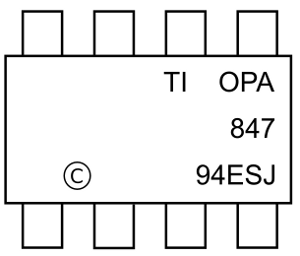
 

The closest marking I found on the link above is the fifth down, yet it is not exactly as shown in my sketch. The copy-right mark is between what I thought to be pins 1&2 and not exactly above pin 1 as one would expect. Also, the (C) mark of itself is somewhat strange since it is not a full white dot nor an embedded mark into the chip (circular dip). Calls to tech support didn't help much and they agreed that I should assume the (C) is between pins 1 and 2. Since I get such odd behavior in DC offset, I just wanted to ask whether anyone have seen such a thing and maybe I have the pins messed-up?

If anyone has any hints I would greatly appreciate it,

Thanks,

Gideon

  • Hi Gideon,

    I have built an OPA847 circuit on one of our unpopulated demonstration boards (DEM-OPA-SO-1B) and have not seen this issue.

    Are you seeing this behavior on your own PC board or on a DEM board? If you are seeing this behavior on your own board, I would recommend depopulating the OPA847 and checking all the pads for the correct electrical connectivity as there may be an unexpected short or open somewhere on your board. A saturated positive or negative output would lead me to believe either the gain setting resistors may have the wrong values or are not connected properly (resulting in a really high gain that is causing any small input offset to saturate the output).

    Another quick thing to check would be to probe the supply pins when the device is powered to make sure that the right supply voltages are at the right pins.

    As shown in Figure 1, do you have the 50ohm resistor to ground? The resistor pulls the input to ground when you leave the non-inverting input disconnected and also provides a path for the DC bias currents of the non-inverting input.

    Are you using +/-5V supplies? -4V is beyond the typical output swing of the OPA847 with +/-5V supplies. Does the output change when you apply a positive voltage at the input? In other words, is it truly an offset and the output still changes with changes on the input?

  • Hi Kristoffer,

    Thanks for your reply. I am using a home-brewed 4 layer board. +/-5V supplies are working fine. I intended to use a relatively high resistor to ground

    at the input to load a photocurrent ( and essentially have a higher bandwidth TIA). That caused an impedance mismatch seen by the input bias currents. Instead of

    the 50ohm I had a 3K loading resistor. When I tested with the 50ohm, the DC offset disappeared. Thanks for your reply. One quick question,

    Eq. (9) shows a noise model for the OPA847. Can you confirm that E_NI 0.85nV/sq(Hz), I_BN=I_BI=19uA and in Eq. (11) I_B=100nA?

    Thanks again.

    Gideon

  • Gideon,

    The currents I_BN=I_BI=I_B in equations 9 and 11 are all equal to the input current noise density, which is listed in the datasheet to have a typical value of 2.5pA/rt(Hz).

  • Of course. Thank you very much.

  • Hi Kristoffer,

    Thanks for your reply. I am using my own board and not the DEM. All points you mention have been checked. The issue was probably DC bias currents. I originally had a 20V/V configuration with Rf and Rg as in the data sheet. My application has actually a large resistor (~1Kohm) instead of the 50 to ground which caused a large impedance mismatch between the inputs. I swapped my Rf and Rg to match (i.e. Rf | | Rg) my large resistor to ground and that helped a lot. 

    Thanks,

    Gideon