Because of the holidays, TI E2E™ design support forum responses will be delayed from Dec. 25 through Jan. 2. Thank you for your patience.

This thread has been locked.

If you have a related question, please click the "Ask a related question" button in the top right corner. The newly created question will be automatically linked to this question.

INA143: can I make the gain of INA143 smaller than 10?

Part Number: INA143
Other Parts Discussed in Thread: INA146, INA821, INA828, INA188

Hi,

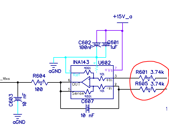
Can I make the gain of INA143 smaller than 10 by adding two resistors at the input side, seen below? I need the gain is around 7. If so, what is the bandwidth at G=7?

I also found INA146 is a OPA with gain adjustable, but the bandwidth is 50kHz at G=1. How about the bandwidth at G=7?

Thanks,

Hongmei

  • The schematic doesn't show in the first message. Here it is. Thanks!

  • Hi H,

    Can I make the gain of INA143 smaller than 10 by adding two resistors at the input side, seen below? I need the gain is around 7. If so, what is the bandwidth at G=7?

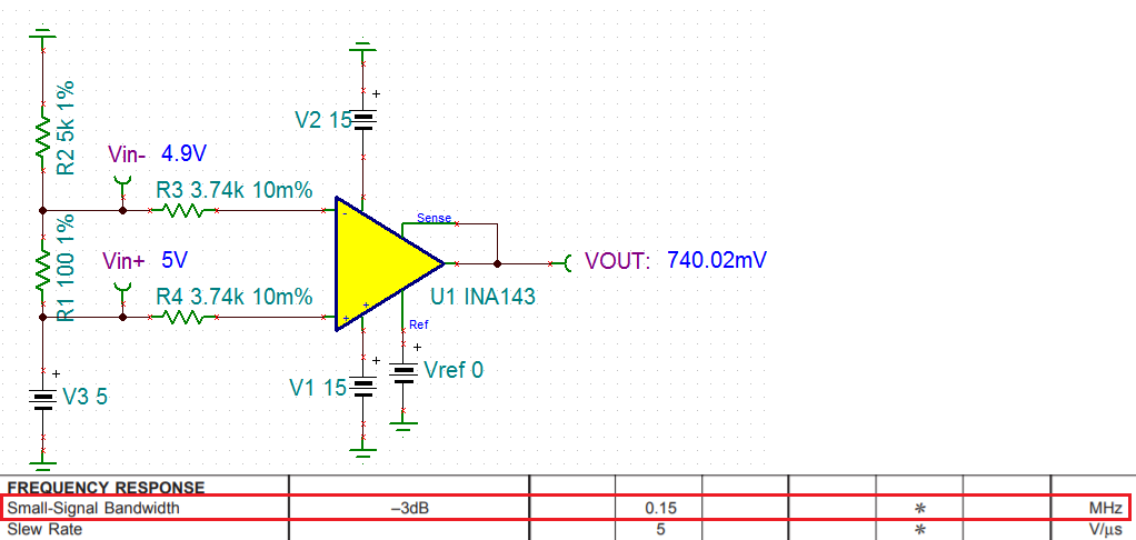
    If you want to alter the fixed gain in INA143, you may use the following configuration. However, you have to use matching resistors or use 0.1% of better resistors in 3.74kOhm. 

    If the Gain=0.1V/V, f_-3dB = 150kHz --> then GBP = 15kHz,  then Gain = 10 V/V, f response at -3dB = 1.5kHz. 

    for Gain = 7, then f response at -3dB = 15kHz/7 = 2.14 kHz. 

    Enclosed is the Tina simulation of the above circuit. 

     /cfs-file/__key/communityserver-discussions-components-files/14/INA143-E2E-08312020.TSC

    I also found INA146 is a OPA with gain adjustable, but the bandwidth is 50kHz at G=1. How about the bandwidth at G=7?

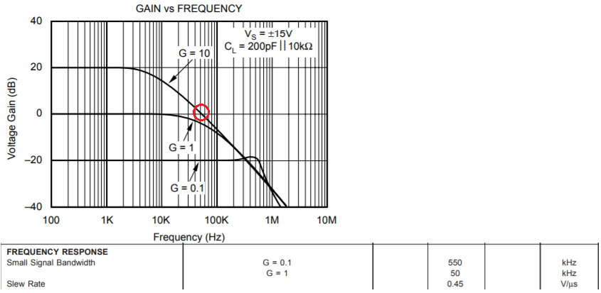
    On p.2 of INA146 datasheet:

    At Gain=0.1, f @-3dB = 550 kHz --> GBP = 550 kHz*0.1=55 kHz,

    At Gain = 1 V/V, f @-3dB = 50 kHz.

    At Gain = 10 V/V, f @-3dB = 5 kHz, 

    At Gain = 7 V/V, f @-3dB = 7.14kHz (assume GBP = 50 kHz)


    Best,

    Raymond

  • THANK YOU very much for your explanations and simulation file,  Raymond!

    INA146UA/2K5‎ has higher BW and no need to consider the resistor requirements. Could you please help me correct the following circuit? Is 1% resistor fine? The differential input is 0-2V. I have 22 sensing circuits using this IC and two boards, one with single +15V, another with dual +-15V. 

    For the power supply, the datasheet (INA143 or INA146) says it can be dual or single. Does it have better performance with dual power supply? Datasheet always shows the application note with dual power supply.


    Thanks,

    Hongmei

  • Hi Hongmei,

    If you are looking for higher BW instrumentation amplifier, we have wide selection of these, see the link below. INA828 & INA821 are low cost and high performance IAs.  What is your design application?

    https://e2e.ti.com/support/amplifiers/f/14/t/818894

    https://e2e.ti.com/support/amplifiers/f/14/t/891120 (not related to your inquiry, but it is a good reference to have). 

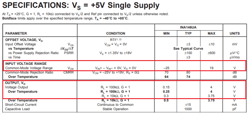
    For the power supply, the datasheet (INA143 or INA146) says it can be dual or single. Does it have better performance with dual power supply?

    You need to check for your input Vcm and Vocm ranges for single supply voltage uses in your application, which it is required to keep the voltage range within the datasheet in order to have a linear response. The input and output voltage ranges are less stringent in dual supply voltage rails (the datasheet only presented +5V and dual supplies). 

    If you have +/-15V onboard, then I do recommend to have dual supply rails. 

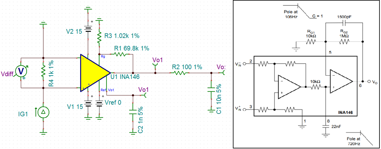
    R2 and C1 LPF may be optional, since I placed C2 at pin8 with cutoff frequency at approx. 15.9kHz. Also, I reduced R1 and R3 values to lower the thermal noises in the circuit. 

    Enclosed is the Tina simulation. 

    /cfs-file/__key/communityserver-discussions-components-files/14/INA146-E2E-09012020.TSC

    Please let us know if you have additional questions. 

    Best,

    Raymond

  • Hi Raymond,

    Thank you very much for your information and I will study INA828 & INA821. I want to amplify the signal to be 7 times larger because I use 15V power supply (originally it was amplified 10 times and the power supply is 24V). This signal is from VOUTP and VOUTN of AMC1311B for DC voltage sensing.

    Thanks,

    Hongmei

  • Hi Hongmei

    INA188 is a good one. It will likely meet your requirements, and pricing is comparable or slightly lower than INA821. 

    https://www.ti.com/lit/ds/symlink/ina188.pdf?ts=1598995968096&ref_url=https%253A%252F%252Fwww.ti.com%252Fproduct%252FINA188

    Best,

    Raymond

  • Thank you for your help, Raymond!

    How about the power consumption of RG in INA188?

    P_RG=[(V+)-(V-)]^2/RG?

    Single power supply 24V, If G=10, RG=5.49k, then P_RG=24*24/5.49k=0.15W. It seems too much.

    Thanks,

    Hongmei

  • Hi Hongmei,

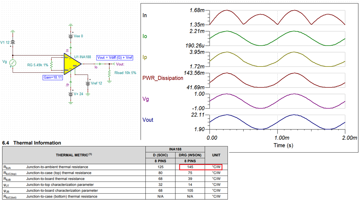
    Here is the total consumed power and power dissipation of the INA188. The peak power is approx. 0.144W and INA188's power dissipation is less, the low peak value is approx. 42mW (It is the sink current at the output will be considered as part of  the INA188's heat dissipation). 

    Let us assume that the INA188 consumes 0.15W, then the IC will increase approx 145C/W*0.15W = 22C from Tamb. The increased temperature is above Tamb or the INA188 will be operating at 25C+22C = 47C at room temperature. What is the application nominal operating temperature?

    /cfs-file/__key/communityserver-discussions-components-files/14/INA188-E2E-09032020B.TSC

    Best,

    Raymond

  • Thank you Raymond,

    It will be in a sealed case and the cold plate for MOSFET device is 65C. I am not sure if the ambient temperature is 65C or not.

    Is RG=(5.49k, 1%, 0.125W) fine?

    Thanks,

    Hongmei

  • Hi Hongmei,

    Is RG=(5.49k, 1%, 0.125W) fine?


    It will be fine. Since you have a cold plate, please use thermal conductive epoxy to bond the INA188 to the cold plate (pot the entire IC to the cold plate) , and make sure that the thermal bonding covers large surface area . The cold plate will have a constant temperature, and the thermal conductive epoxy will transfer the thermal energy to the cold plate, and keep the bulk of INA188 cool (similar to Mosfet's surface). 

    What is cold plate temperature? Even cold plate is maintained at temperature of 65C, 22C temperature rise in the IC will be likely ok, since the cold plate has large mass, and kept at a constant temperature --> generated heat from INA188 will be transferred to the cold plate and will likely maintain the bulk of INA188 to a temperature that is close to 65C. 

    Best,

    Raymond