A related question is a question created from another question. When the related question is created, it will be automatically linked to the original question.
If you have a related question, please click the "Ask a related question" button in the top right corner. The newly created question will be automatically linked to this question.
Michael's request is right. We need to see the circuit schematic to understand why you are getting the unexpected OPA188 Bode plot results.What instrument are you using to make the measurement and how is it connected to the OPA188? It looks like there may be a resonance with the setup around 1 MHz.
You can't ask the output to approach ground, these RR outputs all require some headroom - often, the input can go to ground but in unity gain that is not the limit,
The simulated gain of 1 SSBW often does not match "measured" data sheet plots for several reasons,
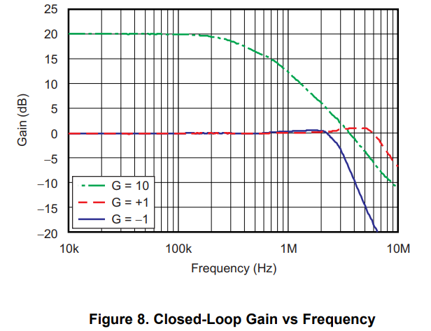
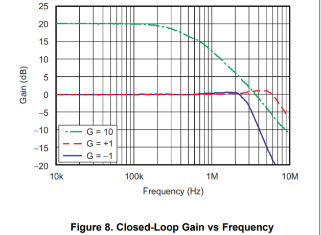
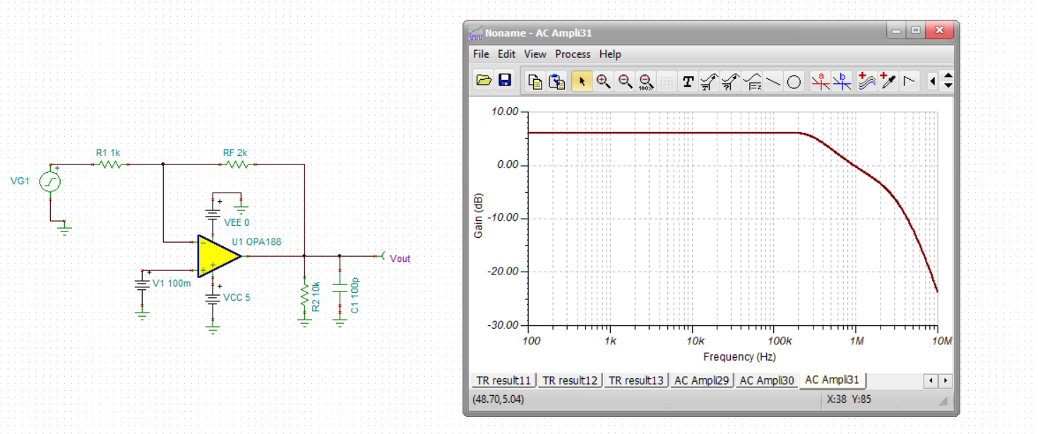
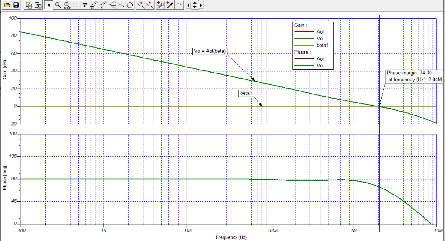
The red curve is what we are looking at here, about 6MHz SSBW gain of +1. But, this has 10kohm in parallel with 100pF load defined - that CLoad is often used to extend the bandwidth by reducing the phase margin,
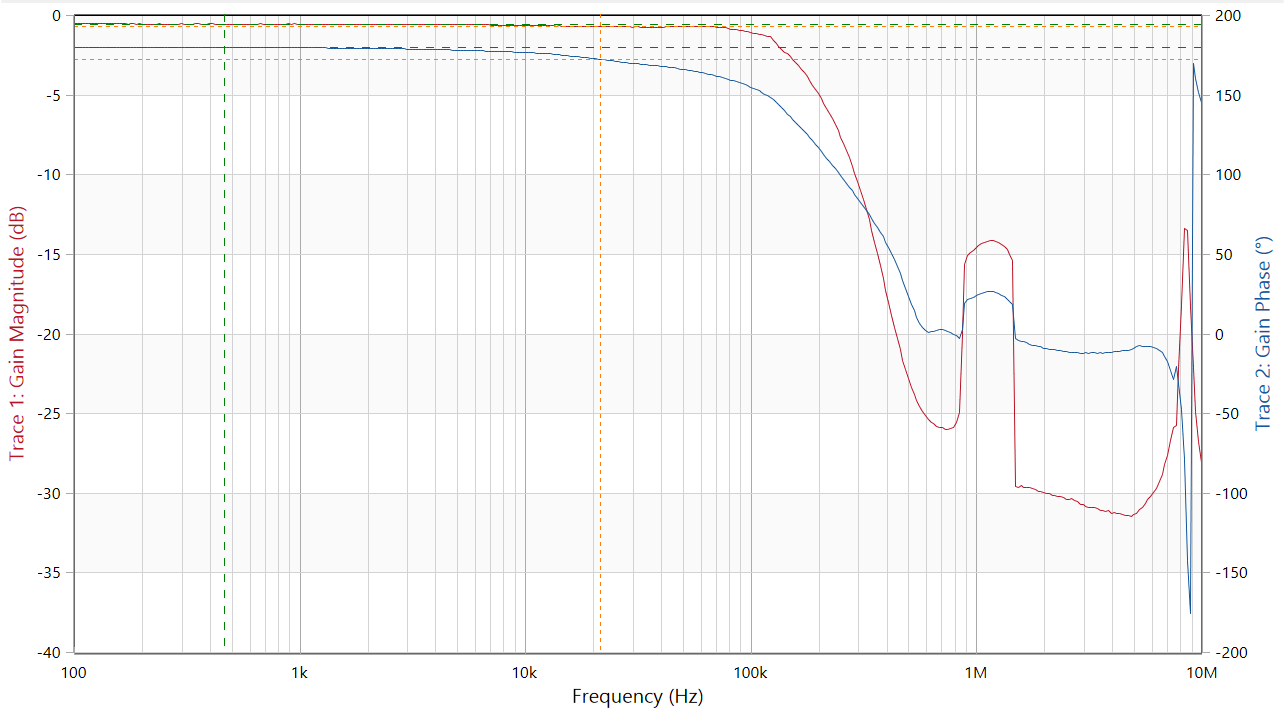
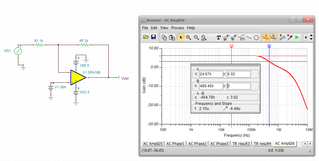
If I rerun your circuit with that load, I get this, that is really off, model must have very poor Aol match to the device, but actually, this is supposed to be a 2MHz GBP part, at noise gain of 3, that measured plot looks way off. Should be <1MHz. Might have put in a curve from a different part. not much change here, about 500kHz F-3dB.
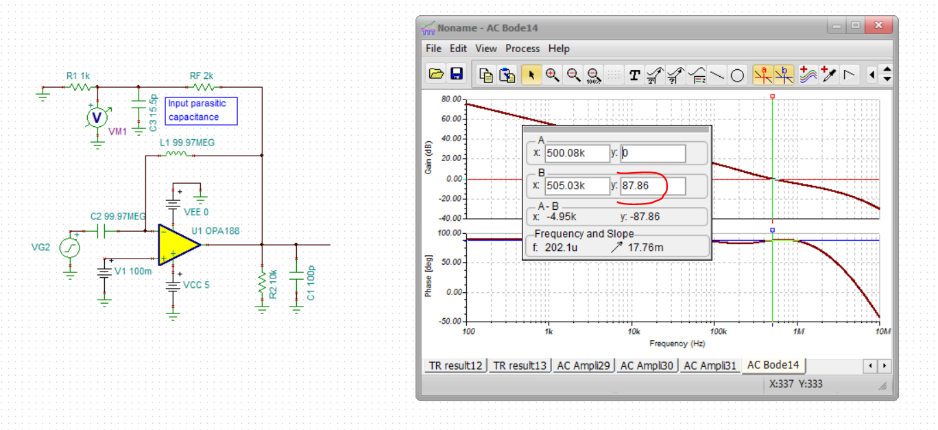
If I run a LG on this ng of 3 circuit, I get this, 500kHz LG=0dB xover with 90deg phase margin? Should be about 500kHz closed loop as the closed loop sim with some DC bias shows. Yes, the measured figure 8 might be from a different part.
When I simulate the OPA188 open-loop gain (Aol) vs frequency using a little different circuit arrangement than Michael used the response agrees closely with the datasheet Figure 7, Open-Loop Gain and Phase vs Frequency graph. The 2 MHz gain-bandwidth product frequency is obtained and the phase margin looks very close.
The Aol simulation circuit was set up with the VCM set to a mid-scale level of +2.5 V, to place the OPA188 input and output at one-half the +5 V supply voltage. The OPA188 output was loaded in the simulation circuit with the 10 kilohm resistor and 100 pF cap to ground as used for the Figure 7 graph.
The OPA188 simulation model is accurate and it includes the correct open-loop output impedance (Zo) vs frequency which is needed for accurate ac simulations. You will need to make sure the OPA188 sees a good circuit representation for the buck converter load if you want good results.
Well yes Tom, I don't think our LG sim approaches should diverge much in this case - your approach isolates the open loop output impedance from the feedback load - makes more of a difference if the feedback has a cap. The reason my LG plot looked different was I was not running an Aol (or NG=1) but a NG=3 test, his application.
I think the question is if the unity gain LG is 2MHz crossover, why does the closed loop plot of Figure 8 show a 7MHz SSBW?
As you know in the AC close-loop output response, there is an interaction between the op amp’s output impedance and input capacitance causing gain peaking that is especially pronounced in low gain – this tends to extend the close-loop bandwidth beyond its theoretical value that assumes a first-order system response. The higher the gain the lower the gain peaking. Having said that gain peaking in a unity gain configuration typically just doubles the theoretical close-loop bandwidth. Thus, I agree that 7MHz is more than one would expect – for this reason, I would question accuracy of the raggedy curve for G=1 - it seems like it was hand-drawn.
Actually, the ideal SSBW extension from LG=0dB crossing for phase margin <60deg is about 1.6X. That, plus a LG sim technique that does not isolate the open loop output impedance from the feedback network, is in this article,
So it would appear this OPA188 plot might be in error in summary.
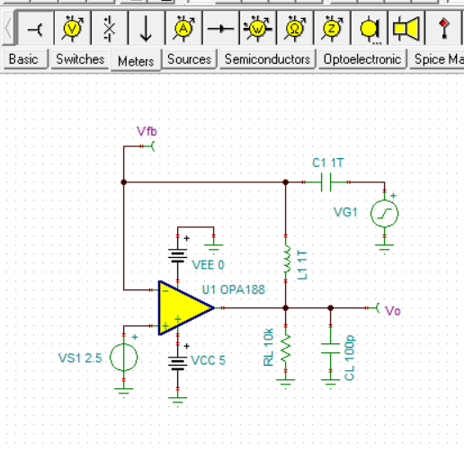
I have attached my OPA188 TINA-TI Spice file for your use.
L1 and C1 are not actual components you would add to your real circuit, but are included specifically for the Bode gain/phase response simulation. C1 provides ac coupling to very low frequencies and blocks dc, while L1 provides a dc current path yet blocks ac. Their use is explained in the TI Precision Labs Op amps series in Section 10 - TI Precision Labs - Op Amps: Stability. You can access the series here: