


Hi to all users!
I have some doubts designing bandpass filter: f0 = 1Hz, Q = 1.41421.
I fount this schematic:
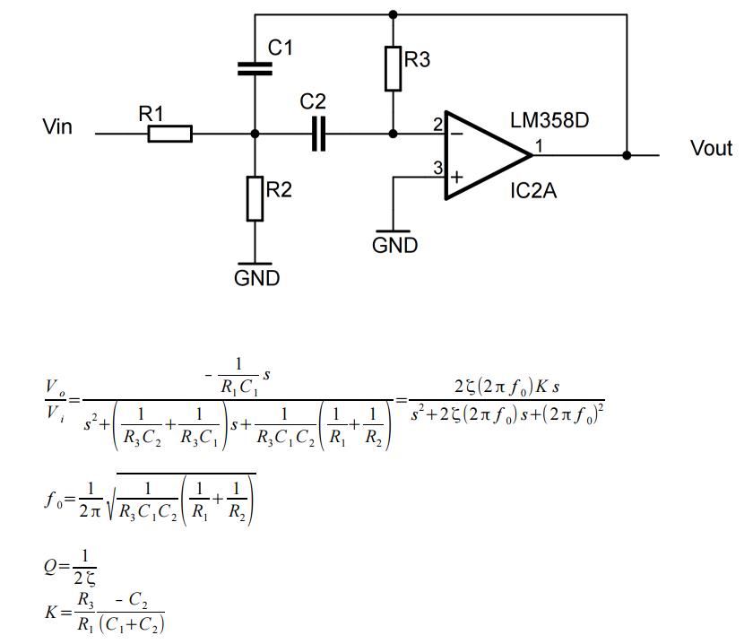
Then I also found slightly different schematic (formulas are given from circuit #1 assuming R2 infinite):

- QUESTION: both gains (if formulas are correct) are not affected by R2 so I can use R2 to trim frequency in first schematic (at fixed gain), while in second schematic if I trim frequency I also change gain. Except this, are there some reasons I should use second schematic instead first one?
In this discussion https://e2e.ti.com/support/amplifiers/f/14/t/354325?Multiple-feedback-band-pass-filter
it's reported slightly different gain formula for second circuit (as I found browsing all around), not talking about C1 and C2 values:
Q = 0,5 * (√R3/R1)
G = -2Q2.
GAIN = -0.5 R3/R1 = -2Q^2
I try to simulate circuit #2 (I have a board with these components):
C2 = 2200nF
C1 = 220nF
R3 = 470k
R1 = 82k
AMP = LT1012
I get different gain, so formula above is correct only when C1=C2. Why I always find C1=C2? Ok, it's more easy, but are there other reasons? I can't undertand why choose different values...
- QUESTION: What about Q when C1 different than C2? Where can I find Q formula explicit for R1, R2, ?
Thanks.


