This thread has been locked.

If you have a related question, please click the "Ask a related question" button in the top right corner. The newly created question will be automatically linked to this question.

AMC1311-Q1: VCMout in different Temeprature and VDD2

Part Number: AMC1311-Q1


Hello,

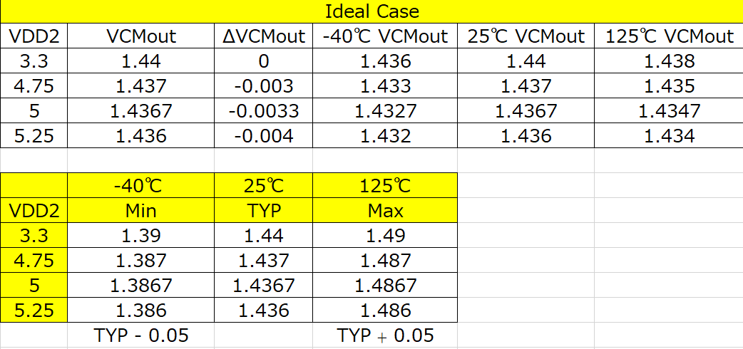
VCMout of AMC1311B-Q1 in datasheet, I see that different temperature and different VDD2 will change the VCMout value.

In the datasheet , the  typical specifications are at TA = 25°C, VDD1 = 5 V, and VDD2 = 3.3 V

the range is 1.39V to 1.49V , so is that means -40 degree / VDD2 = 3.3V    ==> VCMout = 1.39V

but in the follow picture shows that TA = 25°C, VDD1 = 5 V, and VDD2 = 3.3 V ==> VCMout range is about 1.437V to 1.441V

so how can calculate the different VCMout in different Temperature and VDD2? Is there have a formula to calculate?

I want to know about 4.75V to 5.25V / -40 degree to 125 degree   of VCMout

Thanks

  • Hi,

    Can you please re-post the pictures as they did not come through correctly? 

  • Hi, 

    There is no equation to calculate what the common-mode output voltage will be. The variation from 1.39V to 1.49V is due to manufacturing process variation and as such the output common-mode voltage will vary between 1.39V to 1.49V from device to device. Devices with common-mode output voltages outside of this range are discarded. The min and max values of 1.39V and 1.49V does not correspond to the temperature drift.

    As you've pointed out in the second set of pictures, the output common-mode voltage will change depending on the temperature and VDD2 voltage, but this is due to process variation and cannot be predicted reliably. The graphs show typical performance in regards to changing temperature and VDD2 voltage. 

    Since the AMC1311B has a differential output, the common-mode voltage itself it not very important if you measure the output differentially. This can be accomplished using an ADC with a differential input, or performing a differential to single-ended conversion using an operational amplifier as detailed here: 

    Please let me know if you have additional questions. 


  • Hello Alex,

    I have another question

    1.   In the life cycle time , the tolerance won't out of the range 1.39V to 1.49V?

    2.  In the Figure 34, is that the ideal condition? is the curve the same when VCMout change?

    3. so maybe I can see different VDD2 to find the tolerance , because  

    VDD2 = 3.3V VCMout in 25 degree is about 1.44V

    VDD2 = 5.0V VCMout in 25 degree is about 1.437V

    and VCMout tolerance 1.44V - 1.39V = 0.05V

    so VDD2 = 5.0V VCMout is 1.387V (1.39V)  to 1.487V

    Thanks

  • Hi,

    1. No, it should stay within 1.39V to 1.49V over lifetime. 

    2. These graphs show typical performance, meaning the performance of many devices over multiple lots averaged together. The curve will not necessarily be the same from device lot to device lot. 

    3. This is an interesting analysis but I'm not sure how well it will hold over from device to device. As I said before, it is best to measure differentially, or do a differential to single-ended conversion using an opamp near the ADC input.