This thread has been locked.

If you have a related question, please click the "Ask a related question" button in the top right corner. The newly created question will be automatically linked to this question.

OPA2333P: Removing thermal pad

Part Number: OPA2333P
Other Parts Discussed in Thread: OPA2333

Hi Team,

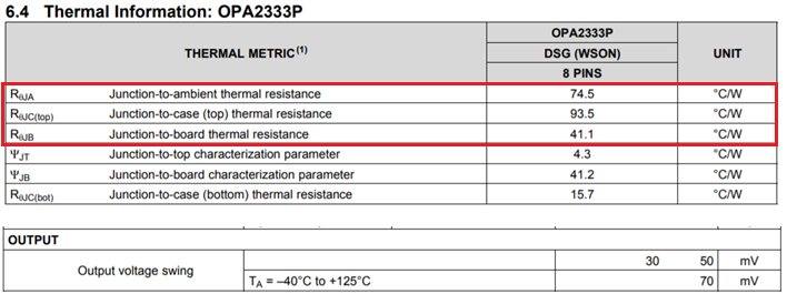
My customer design in OPA2333P in his system, due to PCB is quite small he would like to remove thermal pad then route traces under OPA2333P. Please comment is it doable? Or, is it ok to shrink thermal pad size?

OPAmp drives very small output current to next stage, and it is a portable product supplied by battery. 

Thanks a lot. 

Vincent Chen

  • RθJB will greatly increase, but if the actual power dissipation is small enough, RθJA will suffice.

    But it is not possible to remove the exposed pad from the device itself, and solder mask is not intended for electrical isolation and might contain impurities and holes. Making the PCB under the device available for other traces would require a device in a different package, e.g., OPA2333.

  • Hi Vincent,

    I concur with Clemens recommendation, and WSON package is only 2-mm × 2-mm in size. 

    If you have additional questions, please let us know. 

    Best,

    Raymond

  • Hi Clemens, Raymond,

    Sorry for I didn't express my question clearly.

    Customer wants to remove the thermal pad of footprint on PCB. Then they can rough traces underneath the device. Is it OK since the power dissipation is very small.

    Thank you very much.

    Vincent Chen

  • There is probably not a power dissipation problem.

    But the traces underneath the device might be shorted to the exposed pad.

  • Hi Clemens,

    Thanks a lot for the advice. Like you worried, the space between pads is very small even removing footprint's thermal pads. I will remind customer this point.

    Vincent Chen

  • Hi Vincent,

    Please calculate the power dissipation on the OPA2333P and verify the temperature rise per the table below under the worst application operating condition. Thermally it is likely ok, if you remove the PCB's thermal pad, and replace it with a ground or the most negative potential on the PCB. 

    Electrically, there are micron spacing or gap between the exposed ground lug and soldering mask. I don't know the types of traces you are going to place underneath. There is a chance that ground lug can short through soldering mask to traces underneath, since mask is not intended for electrical isolation (quality of soldering mask, dusts, mask thickness and uniformity, micron holes in the mask, moisture, temperature etc. may play roles in the real world operation).  These are possible potential risks that may affect the function of  the op amp and final product. It is doable, but I would not recommend it, especially if it is in a critical application.

    Best,

    Raymond 

  • Hi Raymond,

    I got your point, I will explain it to customer and ask him to keep PCB's thermal pad.

    Thanks very much for you guys help.

    Vincent Chen