This thread has been locked.

If you have a related question, please click the "Ask a related question" button in the top right corner. The newly created question will be automatically linked to this question.

AMC3330: Using Multiple Parts on top/bottom Layout

Part Number: AMC3330

Hello,

We need to use multiple AMC3330 parts placed TOP/BOTTOM on a layout due to limited space.

There is a concern that the DCDC noise from the top device will interfere with the analog performance of the bottom device, and visa versa. Will this be a problem?

The data sheet shows that there should be no ground plane or any copper located under the package, but in our case of the TOP/BOTTOM layout would it be a recommendation to have a shielding plane between the top and bottom parts?

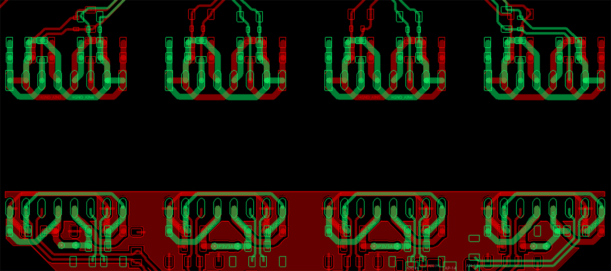
Here is an idea of how we have the placement now. Red = top, green = bottom. The top/bottom AMC3330 pins coincide exactly.

Any help greatly appreciated!

Thanks, Ken

  • Hi Ken,

    only the experiment can fully answer this question, I guess :-)

    Kai

  • Hi Ken,

    I spoke with the design team and our recommendation as a precaution is to not overlap the top portion of the devices (pin 1-4 & 13-16)  as it contains the internal DC/DC converter. The signal chain portion of the devices can overlap on top/bottom layers of the PCB without issue. This would allow for some space saving while also ensuring correct operation of the DC/DC converter. 

  • Hi Alex,

    Thanks for the reply and recommendation.

    As a compromise could we consider overlapping the DCDC section with DCDC of the adjacent bottom channel?

    That is, move the bottom layer to the right by half of a package.

    This way the signal chains will overlap and the DCDCs will overlap.

    Sorry to ask, but we are really pressed for space.

    Thanks, Ken

  • Hi Ken,

    a shielding ground plane between the top and bottom layers should definitely help. But, of course, don't violate the safety gap.

    Kai

  • Hi Ken,

    I think keeping it spaced apart as I wrote earlier is best, but overlapping DC/DC's and signal chain's as you've mentioned would be preferred to the configuration shown in the OP. Since the noise in your system is specific to your system, as Kai said, it is difficult to know for sure what the impact will be without testing. 

    Is this project going to undergo EMI or EMC testing? If so, we do not recommend a ground plane on the high side of the device. 

  • Hi Alex,

    Thanks for the further comments. We will continue with the layout overlapping the signal chains and there will be a portion of the DCDCs that overlap as well.

    Yes, there will be EMC testing, so thanks for the tip about the high side ground plane. I was not going to have one, but good to know.

    Best regards, Ken

  • Hi Alexander,

    Is this project going to undergo EMI or EMC testing? If so, we do not recommend a ground plane on the high side of the device.

    That's indeed important information! Thanks :-)

    Kai