This thread has been locked.

If you have a related question, please click the "Ask a related question" button in the top right corner. The newly created question will be automatically linked to this question.

OPA189: Do SPICE models implicitly reference GROUND

Part Number: OPA189
Other Parts Discussed in Thread: TINA-TI, INA149, LMP8480, OPA388

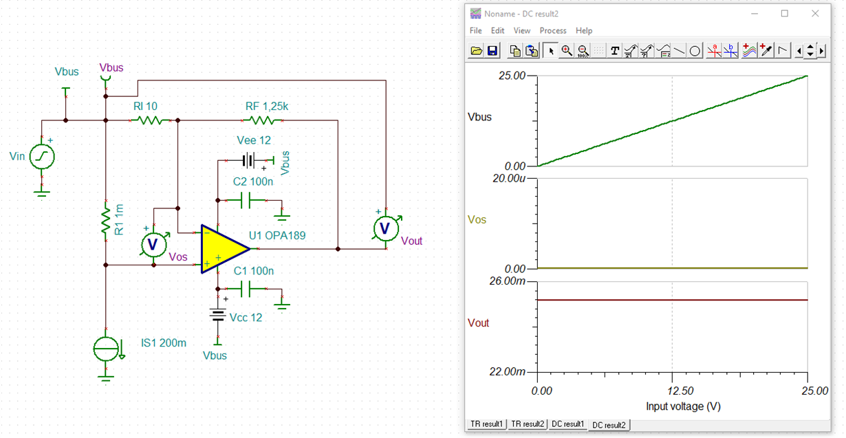
I am working on a design for a high-side current monitoring circuit, using an OPA189.  A very simplified schematic is shown below.  I have simulated this simplified schematic to confirm it generates the behaviors I am about to describe.

The OpAmp receives floating +/- 12V power, and the entire circuit sits at voltage Vbus.

When Vbus = 0V, the circuit performs as expected.  As Vbus increases from 0V to 24V, performance worsens.  The signal at OUT increases from less than 0.1% error, to over 5% error (closed loop gain = 125).  When Vbus = 50V, the simulator I am using refuses to complete the simulation. 

My observation is that Vofs reported by SPICE (I probe the delta between (+) and (-) input pins) grows larger and larger, well beyond the datasheet limits, as Vbus increases.  Note there is no explicit connection between the OpAmp and GND.  VCC and VEE appear to be +/- 12V relative to the common-mode input signals.  In this simulation, the voltage across Rsense is a few millivolts.  Therefore the common-mode input that the OpAmp sees is for all practical purposes perfectly centered between VCC and VEE.

My assumption is that the op-amp SPICE model has internal references to the global GROUND node [notionally V(n000)], and does not perform as expected when floated to some arbitrary voltage away from ground.  Can someone confirm this to be the case?

Thanks,

Will

EDIT: Changed "Vsense" to say "Rsense"

  • Hi Will,

    have you already carried out a simulation using TINA-TI? Does it show the same behaviour?

    Kai

  • Kai,

    I generated the same example in TINA-TI, and I get the same results.  .TSC file included here.

    Thanks

    Will

    sbomaf0c.tsc

  • Hi Will,

    thanks for the simulation file! This saves a lot of time :-)

    Well, the TINA-TI's "DC Transfer Characteristic Analysis" shows a different result:

    will_opa189.TSC

    Kai

  • Kai,

    Thanks - I have never used the DC Transfer Characteristic in TINA-TI.

    I downloaded your TSC file (thank you) and of course when run using DC Analysis, I obtain the results you posted.

    Do you agree however, that when using the Transient analysis, the problem does exist?  The schematic I provided is a very simplified example.  I cannot use the DC analysis to simulate the final circuit I am trying to achieve -- I believe it must be simulated using Transient analysis.

    Thanks,

    Will

  • Hi Will,

    Do you agree however, that when using the Transient analysis, the problem does exist? 

    The problem will still be there, because the input is likely outside of the input Vcm mode range in OPA189. Are you sure that you are not talking about INA149, LMP8480 or other high side current sensing op amp?

    https://www.ti.com/amplifier-circuit/current-sense/products.html?pqs=paqs&familyid=3170#p2192=Bi-directional&p0max=12;80&p773=100;75;60;50;25;20&p726max=2;80&sort=p0max;desc

    If you are looking for current sensing amplifier, I can connect you to our Op Amp Current Sense Team. Please let us know. 

    Best,

    Raymond

  • The input is actually centered to within a few mV between the two supply rails.

    I uploaded a TINA simulation file that you can run, and verify.

    The Vofs rating of the high-side current sense amps is too high for the accuracy I am trying to achieve, which is why I'm using this topology.  I have omitted in my example schematic a P-channel mosfet path to ground, which gets the measurement point back down to ground reference.

    I believe I have satisfied myself through further testing that the SPICE model has an issue when floated above ground.

    Will

  • I guess to further clarify... you circled the single supply max rating.  I am providing +/-12V in this case, which is less than the +/-20V allowed.  There is no ground pin on the op-amp.  It only knows about the voltages present at the V+ and V- input pins, and the two supply pins.  The fact that the whole thing is floated up to 50V, the op-amp won't know any different than if it was at 0V.  But the SPICE model does seem to assume that the voltages are centered around 0V, and generate false errors when the entire assembly is floated to some arbitrary voltage.

  • Hi Will,

    Ok, I see what  Kai did with Vbus. You are running boostrap mode in OPA189.

    You mentioned "I uploaded a TINA simulation file that you can run, and verify." Are we talking about the same simulation file?

    Let me simulate the transient conditions and get it back to you. 

    Best,

    Raymond

  • Raymond,

    My post Nov 26, 2020 9:49 PM had sbomaf0c.tsc attached.


    Will

  • Hi Will,

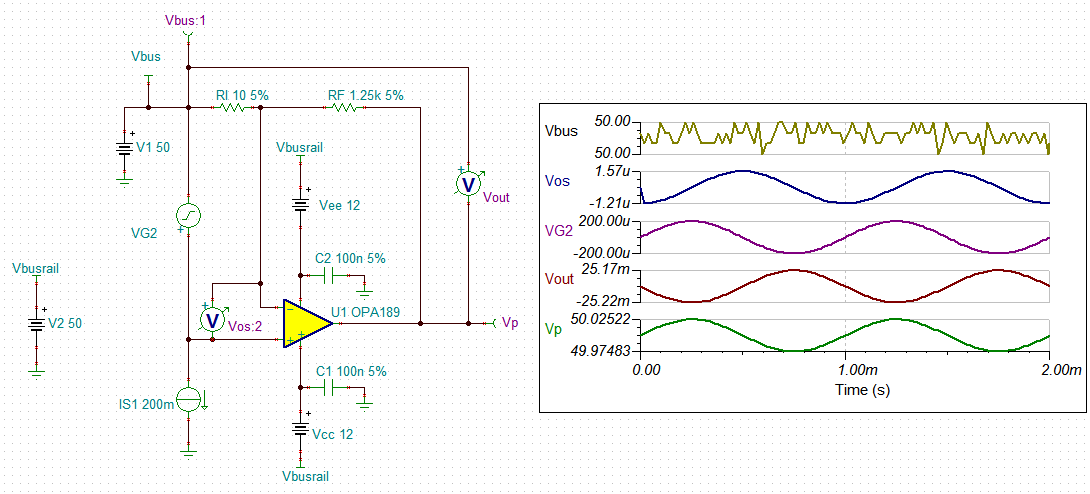
    I simulated the following circuit, but I am not sure if this is what you want to see. Please let me know. 

    With 1mOhm sensing resistor and 200mA current, I inserted VG2 in sinewave with +/-200uV amplitude. 

    /cfs-file/__key/communityserver-discussions-components-files/14/Will-OPA189-E2E-11302020.TSC

    200mA constant current is high impedance source. The input nodes are floating. I change the impedance of IS1 to 1Meg from infinity (or make no difference). 

    BTW, if you want to increase the display resolution, right click on a selected vertical axis, left click on the axis property, then change precision from 2 to high value. 

    Best,

    Raymond

  • The simulation I had setup in the original TSC file I uploaded showed the error I was trying to demonstrate.  In this case, I'm not worried about AC performance, per  se.  In the file I uploaded, see the Vofs plot.  Depending on the voltage level of Vbus, Vofs changes.  This affects the effective DC gain of the amplifier.  By Vbus=25V (or 50V, I forget), at a DC gain of 125 or so, the output error becomes over 5%.  The 200mA across Rsense is generating the same delta-v across the inputs, and the resistor-programmed gain isn't changing.  Therefore, the output voltage (and Vofs) should remain the same.  But they do not.

    I am simply hoping that someone from TI can confirm the error is caused to the input nodes of the SPICE model referencing global ground (node 000).  

  • I gave myself a quick primer on spice netlist format, and examined the OPA189 spice file.  There are numerous components tied directly to node 0. 

    This satisfies my question, that the spice model does have fixed references to global ground node 0, and therefore cannot be simulated properly in a floating situation.

    I'm not sure why I didn't just examine the spice file in the first place.  Leaving the thread up for others searching with the same question / problem.

    Will

  • Hi Will,

    all these simulations are only valid for plain standard operation with constant supply voltages, input voltages not leaving the supply rails, etc. The models are not really simulating the true chip behaviour but are highly simplified. A true chip simulation would need a super computer to make the simulation run :-) So we have to live with simplified and sometimes even highly simplified models which nevertheless can show true results and do definitely enormeously help in the designing phase. But we have to accept some restrictions and have always to keep in mind that the simulation will never tell the whole truth. That's the deal. :-)

    Kai

  • Yup I understand of that. 80% of the time I spend doing simulations is figuring out what's valid and what's a simulation artifact.

    That said, there is an op-amp vendor who uses a different method to generate their SPICE models, which does not have embedded references to node 000, and therefore can be floated without affecting the accuracy of the model.  There is a white-paper out there on the topic. 

    This is why I asked the question originally... because it's not immediately clear how each vendor creates their models.  I was trying to be sure the errors I was seeing were due to operating with a bias offset from ground (Vbus floating up) and not coming from some other source, which could have been modeled correctly, and would be something I would need to correct / account-for in my design.  In other words, yes the models aren't perfect, but understanding more clearly in which ways they are deficient helps to predict and understand how the circuit will actually operate once tested in hardware.

    Will

  • Hi Will,

    I am pretty certain you have hit the nail on the head. TI's moden op amp simulation model used for the OPA189 is very sophisticated and most electrical behaviors can be replicated in simulation. However, it is not ground (node 0) independent as you have noted. Therefore, when the op amp supplies are floated there is no assurance that the model will be able to maintain correct performance.

    In the cases of the dc performance and sine wave it looks to be okay. But when the transient step conditions are applied we see the offset glitching. That might be because the input common-mode capacitance is node 0 referenced. I do think the dc results you are obtaining with the OPA189 model are believable. I hope that is sufficient to help you assess the operation of your circuit.

    Regards, Thomas

    Precision Amplifiers Applications Engineering

  • Will,

    I was actually able to replicate the same waveform shape even when I changed everything to a traditional dual supply and just measuring a gained up Vos of the amp itself, as a piecewise linear signal was applied to the non-inverting input.  What I noticed (when I reduced the amplitude) was that the DC level after each transient was changing a bit...  I believe what I was seeing there was simply CMRR.  That leads me to believe that likely there is something internal to the model that does interpret your floating circuit as still having a CMRR component being calculated.  It is of course a behavior macro model utilizing voltage dependent voltage sources, non-ideal impedances to assist in convergence, etc.  It is not a transistor level model, and so a bit of imperfect behavior in lieu of simulations that take 1000x as long doesn't surprise me completely. 

    All that said, reviewing your circuit it looks good.  I've done similar things in the test and measurement world, floating +/-5V op-amps on +/-100V common modes, measuring similar things to what you are doing.  Assuming you've got an isolated DC-DC converter riding on the common mode, just be conscientious of AC return current loops, good local bypassing, etc.  And of course if you aren't aware already, TI does offer isolated DC-DC converters, which I used with great success in my project. 

    And of course if you can live with a little more inaccuracy at your lowest current levels, you might be able to do away with the Vbus+X supply altogether if a RRIO op-amp (e.g. OPA388) is chosen.  The Vbus-X supply can be easily generated with an LDO or even Zener+resistor, etc.  

    Good luck!  

    Thanks,
    Scott       

  • Scott,


    Thanks so much for the follow-up reply.  You described the problem I was seeing exactly, and worded it better than I was able to.

    Thanks for the pointer to the OPA388.  It is not too far off from the OPA189 it seems performance-wise (I am seeing 2:1), but for other reasons I am already saddled with a floating supply, so I will probably stick with the topology I already have to keep my error margins minimized.  At the lowest measurement values, I am starting to include leakage current through the PCB material in my feedback loop as a potential source of errors, so I am trying to wring the most out of the op-amp as far as minimizing offset errors it introduces.

    I did look at TI isolated converters, but for reasons I can't recall I down-selected to another vendors part, whose family I used successfully on a 400V project previously.  I can't remember the differentiating factor at the moment.

    Thanks again,

    Will

  • You're welcome Will.  Sounds like you've got it figured out and quite a precise circuit to deal with.  If you have any questions regarding your implementation that aren't suitable for a public forum (e.g. sharing schematic), feel free to PM me.  Take care.