This thread has been locked.

If you have a related question, please click the "Ask a related question" button in the top right corner. The newly created question will be automatically linked to this question.

OPA454: Feedback resistor value, unity gain buffer

Part Number: OPA454
Other Parts Discussed in Thread: TINA-TI

Hello team,

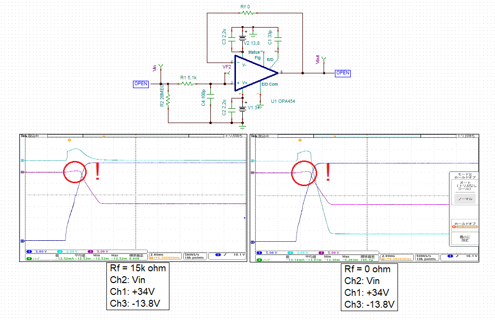
My customer is evaluating OPA454 with unity gain buffer configuration. Please see attached tina-ti file for schematic.

0636.OPA454.TSC

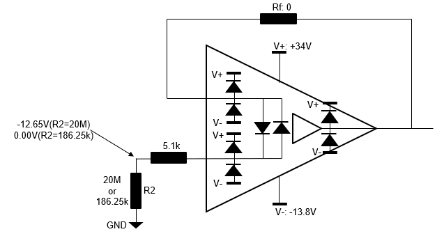
Non-inverting input is tied to GND through 20Mohm, so customer expected the input voltage to be 0V. However customer observed -12.6V at input(Vin node) when Rf is 0 ohm. Changing Rf value to 15k ohm makes input voltage 0V as expected.

I would like to confirm below things. Could you let me know below?

  1. Why Vin node becomes -12.6V when Rf=0ohm? 20Mohm is too big?
  2. Why the behavior is improved by changing Rf to 15kohm?
  3. What Rf value is recommended in the case?

Best regards,

  • Sato-san,

    A 20 Meg source resistance is very high and I don't recall ever seeing that used with the OPA454; not to say it can't be. Is the customer seeing the -12.6 V Vin+ voltage with just one OPA454 device, or with any OPA454 they install in the circuit?

    The steady state OPA454 input bias current (Ib) flowing through 20 Meg resistor shouldn't result in the Vin+ input being at -12.6 V. Even if Ib gets up to 100 pA, the voltage drop across the 20 Meg resistor would be only a few millivolts. The behavior might be due to a time constant issue with the input RC (20 Meg and 100 pF), or something happening with the enable/shutdown function such as glitch coupling the E/S pin.

    Here are some things I suggest checking and the results should help guide us to the issue:

    1. Check and make sure that the OPA454 underside PowerPAD is soldered to a PCB pad connected to the most negative supply voltage (-13.8 V). That is an operating requirement to assure normal operation..
    2. Try disconnecting the 100 pF capacitor connected from the OPA454 non-inverting input to ground. See if the voltages at the non-inverting input and output become close to 0 V.
    3. If removing the 100 pF capacitor doesn't resolve reinstall it. Then, try lowering the value of the 20 Meg resistor and see if doing so corrects the issue. If it does, what resistance corrects it?
    4. If the previous do not help, connect a 1 Meg resistor between V+ (+34 V) and the E/D pin as described in datasheet Section 9.3.6 ENABLE and E/D Com. See if that makes a difference.

    It is usually preferable from AC and noise standpoints not to include a feedback resistor in a simple op amp buffer circuit. Oddly, they observing that the Vin+ voltage issue doesn't seem to occur when they include the 15 kohm resistor in the feedback loop. Having the resistor does change the time constant in the feedback loop and that may be countering a time constant behavior occurring in the non-inverting input circuit.

    We will be able to tell more after my suggestions are checked.

    Regards, Thomas

    Precision Amplifiers Applications Engineering

  • Hi Taketo,

    looks like latch-up occurs because your negative supply voltage becomes positive during power up for a brief period: 

    A remedy is discussed here:

    Kai

  • Hello Thomas-san,

    Thank you for your support.

    Customer sees the behavior with not only single unit but two units out of two.

    I confirmed below with customer.

    1. Power pad is connected to V-(-13.8V).
    2. Disconnecting 100pF from non-inverting input --> No improvement
    3. Reinstall 100pF cap and change resistor value -->
      1. 20M ohm: -12.65V
      2. 952.38k ohm: -12.6V
      3. 487.8k ohm: -12.55V
      4. 186.25k ohm: 0V
      5. 99.5k ohm: 0V
    4. Pull up E/D pin with 1Mohm --> No improvement

    Additional info., Customer observes -12.6V at Vin node but they see -13.7V at Vout and VF2 node.

    I would appreciate if you could provide possible cause and a reason why Rf helps the situation.

    Best regards,

  • Sato-san,

    Thank you for running the checks I described. The results indicate that the odd voltage -12.6 V appearing at the non-inverting input is not a normal linear circuit behavior. I think that Kai is correct and the observed behavior is an input latch-up occurring because the two supplies V1+ and V2- are not coming up together as seen in the DSO images. Changing the R2 resistor value changes the amount of input current that can flow and it appears when it can be momentarily higher the latch doesn't form, and the input voltage is near the expected value of 0 V. 

    Kai described the issue in the previous e2e where he stated, "voltage regulators providing a bipolar supply voltage can behave very strange during power-up and power-down, if unequal supply currents are drawn from the both supply voltages. This can make the positive supply voltage become negative or the negative supply voltage become positive, depending on which supply current is higher. This is dangerous not only for the OPAmp but also for the regulators because latch-up can occur. A good remedy is to clamp the output voltages of regulators by the help of a 3A Schottky diode each. Figure 26 from the datasheet of LM7800 shows what I mean."

    When dual power supplies don't come up in unison one remedy that we recommend and often helps is adding either Zener diodes, or Transient Voltage Suppressor (TVS) diodes from each supply pin to ground as shown below. Adding the diodes assures that there is always a power supply current path through the op amp. The Zener or TVS diodes used need to have a breakdown voltage that is higher than the sustained supply voltage levels.

    Regards, Thomas

    Precision Amplifiers Applications Engineering

  • Hello Thomas-san,

    Thank you for your comments. I will have customer consider adding TVS diodes.

    By the way, what do you think why Rf resistance helps the behavior? Do you think 15k ohm as Rf can be also solution? Since they have a footprint for Rf in their board, if Rf could be a solution, it is easier for them.

    Best regards,

  • Hi Taketo,

    you definitely have an issue with the supply voltage generation and you should solve it by adding the Schottky diodes :-)

    Kai

  • Hello Sato-san,

    Evidently including the 15 kilohm feedback resistor helped with the latch condition for the two OPA454 devices evaluated. The concern is if that solution will works for every OPA454 device that would be received in the future.

    Inclusion of the 15 kiloohm resistor in the feedback loop will have some effect on the phase margin. If the circuit is stable with the required output load in place and its not showing any excessive ringing with the resistor in the circuit, then it should be okay to include it.

    But please do consider Kai's suggestions.

    Regards, Thomas

    Precision Amplifiers Applications Engineering

  • Hello Thomas-san, Kai-san,

    Thank you for suggesting input latch-up due to power supply sequencing.

    However OPA454 datasheet Figure 54 states "Power supplies may be applied in any sequence".

    1. Why does this customer case require power sequence?
    2. Is it correct that power sequence could be a only cause of the latch-up and any input voltage doesnt cause latch-up as long as used in recommended operating condition?

    Also, could you let me know why high input source impedance forms latch-up but low input source impedance doesnt form latch-up?

    Explanation with block diagram(like below) would be helpful.

    Best regards,

  • Hi Taketo,

    this has nothing to do with power sequencing. And this has nothing to do with the OPA454. But it is a problem of your supply voltages.

    A positive supply voltage starts from 0V and settles to the final (positive) value without ever going NEGATIVE. A negative supply voltage starts from 0V and settles to the final (negative) value without ever going POSITIVE. But your negative supply voltage is violating this rule! For a brief moment the positive supply voltage is positive AND the negative supply voltage is POSITIVE:

    This means that the input voltage of OPA454 (0V via R2) falls outside the allowed input voltage range at this moment which is very very very bad design practise :-(

    It's pure coincidence that the OPA454 recovers from this torture with the feedback resistance mounted and does not recover without the feedback resistance. And it's an entirely incorrect conclusion that the feedback resistor cures this mistake :-(

    Please cure the supply voltage generation by adding the Schottky diodes.

    Can you show a schematic of your supply voltage generation?

    Kai