This thread has been locked.

If you have a related question, please click the "Ask a related question" button in the top right corner. The newly created question will be automatically linked to this question.

THS4631: settle time

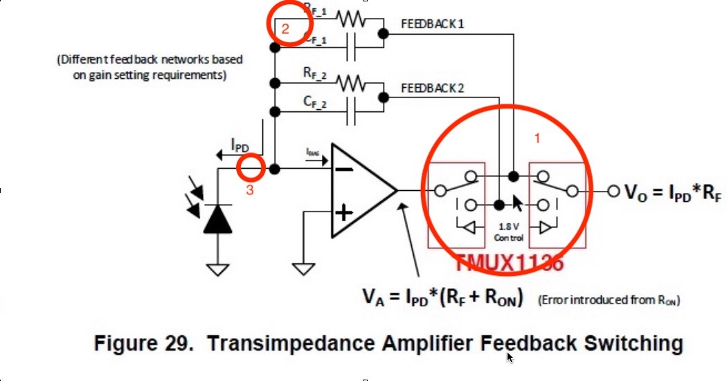
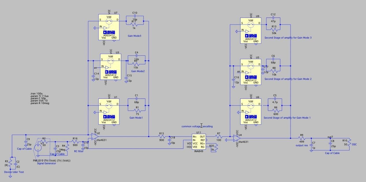
Part Number: THS4631
Other Parts Discussed in Thread: OPA810, OPA857, LMH32401

Hi sir,

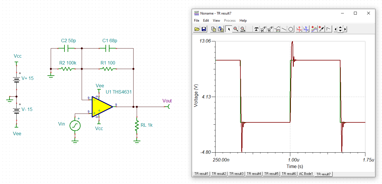
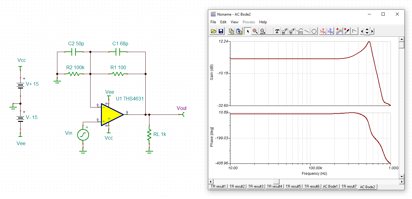
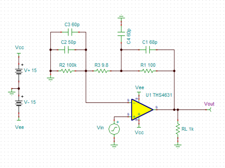
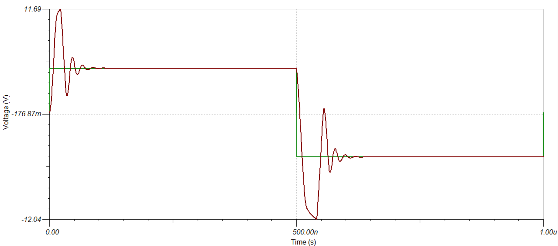
I have a technical problem on ths4631.

when testing the output port,
the difference between the test value of 1us and that of 51us is 14uv.
How to modify the circuit so that the output can be stabilized to 0.6% DD of the stable output within 500ns.
Thank you for your suggestion.

  • Hi Frank,

    because of the big C2 the circuit isn't stable:

    frank_ths4631.TSC

    What is the maximum variation range of your R3 and C2?

    Kai

  • Well Frank, aside from Kai's point on stability - 

    1. Are you really using a switch in the feedback (ADG5412) if so, 

    a. If you are opening closing this, is that not opening the feedback loop and then reclosing it? that is not modeled well

    b. you need to include its parasitic C in your sims. 

    2. Your question on the small shift in voltage over long time? Is that a sim or a bench measurement, if a bench measurement, that is long term thermal tail - almost no one pays any attention to that anymore, but I used to test it for the Comlinear op amp intro's. Not going to fix it nor find a newer part specifying it. In any case, you should be aware of the much newer OPA810 JFET high speed part, not to say that it would be better on thermal tail, but might be on other things. 

  • Hello,

    In addition to Kai's comments it is worth noting the effects of your switch which will make it very difficult to stabilize this circuit. The spice model for the ADG5412 seems to only include the capacitance when device is off (18pF) but in reality this increases significantly to 60pF on both sides of the switch when the switch is turned on (60pF). Note the following sims:

    Best,

    Hasan Babiker

  • Hi Hasan, Michael, Kai,

    Thank you for your response and professional analysis.

    Firstly, It will be better that i give a rough description about background and what I am doing currently.

    1. It is a typical TIA application. R1 is the Gain Res. C2 is parasitic capacitance And C1 is used to compensate the inadequate phase margin caused by C2(a zero point in 1/ß network). U1 is used to change gain of this circuit.

    2. R3 represent as a resistance load along with some intrinsic Cap(including parasitic capacitance of coaxial cable 100pf/m, stray parasitic capacitance of PCB), So i make a rough assumption that C2 is around 50pf.

    3. In short, i want to measure the current flow pass the R3. the current may be 10mA range to 10nA. This is the reason why i used a analog switch U1 in this circuit which can be used to select suitable gain. Fortunately, once work, the current is fixed, and i can change the Gain during the TIA is not outputting.

    4. What is different between my circuit and TIA application is that usually a PD(photo diode) is connected to inverting-node of OPA, and the non-inverting-node of OPA is tied to a fixed voltage level. But in my case, there will be a pulse (with certain Tr and Ton) trigger/enter the non-inverting-node of OPA. And the R3 will act quite similar to PD which as a current source.


    So, i hope making a brief introduction about the background. Then come to the issue.

    1. R3 represents a resistive DUT which may be 1k~10meg omhs. But we can more interested in the current flow pass it, maybe 10mA~1uA.

    2. C2 is around 50pf in worst case.

    3. As the simulation done by you shown, the C2(parasitic capacitance ) is catastrophe to the stability of TIA circuit, but i cannot remove this side effect. The drifting of output in 50us scale is perhaps due to ringing. But how can i enhance to typology of this circuit to reduce the ringing? I know the overshoot and Q factor can represent the phase margin. So maybe the correct question is how to improve the phase margin.


    Thank you for your patient reading and focusing on my problem.

  • Hi Frank,

    so the detector capacitance of photdiode adds to the 50pF at the -input of OPAmp?

    What is the detector capacitance?

    Kai

  • Dear Michael,

    Thank you for reminding the switch(ADG5412), and i haven’t paste the entire circuit and this may confuse you. And my reply to Kai maybe can help you have a better understanding about my circuit and issue.

    1. a. the switch is used to select different Gain of TIA. There is another switch and Rf/Cf in the circuit.

    2. b. When i choosing the analog switch, i considered the parameter Con Coff Ron I_leak. The Spice model is from manufacture(your competitor ). to be frank, how to confirm that the Spice contain the parameter which i really concern about (Con Coff Ron I_leak). maybe just the method used to test the Ccm and Cdiff of OPA, measure the f-3db of RC effect.

    2. the drift is a sim. As for OPA810, i checked the datasheet, the parameter is suitable for my case, they are both FET OPA. But the GBP(70M) is weaker than THS463(210M). for 10mA TIA case (R3 is 1k load), the desired closed-loop-bandwidth is 16Mhz for me. And in my case, it seems that the the equation used to calculate the GBP and closed-loop-bandwidth in TIA case is not suitable.

  • Dear Hasan,

    Thank you for suggestion. it comes to me that whether the analog switch is suitable for my purpose which just want to change the gain. Actually, i evaluated the switch in 3 different place, finally the position 2 is the one which can come to steady easiest.

    2. i will double confirm that the Spice mode of analog switch contain the Con and Coff.

    2. Assuming that, if i use a cascade amplify design mode. I am quite worry about the Noise performance (0.2% of output range). it is my common sense that put the gain to the first stage will always attain a better noise performance.

    a)         For the common voltage canceling, the mismatch of Res will lead to Vcm to Vdiff which is not desired. So, do you have any suggestion about how the achieve a differential operation between signals with the same OPA ths4631(GBP and +/-15V power rail limited the choice ). e.g. the highly matched res array.

  • Hi Frank,

    I'm a bit confused now. Can you please show a complete schematic of the first stage? Which also shows how you want to mount the photodiode? And what is the detector capacitance of this photodiode?

    Kai

  • Hi Kai,
    Sorry for making you confused. Here is the complete SCH of my design.

    1. the Device Under Test(DUT) is not a photodiode, but a resistive load with certain mount of parasitic Cap. What we want to do is using the typology of transimpedance OPA to amplify the weak current flow through DUT, Maybe 100nA.

    2. The total Cap which can be saw from the Vin- of OPA is (Cap of Cable)+(parasitic Cap of DUT)=50pf.

    3. The Signal Generator can change the common mode voltage of OPA, which induce to change the voltage applied to DUT.


    Maybe this is hard to understand why we use this method to measure the current parameter. And this is not a traditional case which just use a PD which is mounted in the PCBA. If you still have further question, i am willing to share more with you.

    Thanks.

    Regards,

  • Hello Frank,

    Have you considered using a TIA device with internal switches such as the OPA857 or LMH32401?

    Best,

    Hasan Babiker

  • Hi Frank,

    and you need to measure with a 1MHz square wave? A DC measurement or an AC measurement with a much lower measuring frequency wouldn't do?

    Kai