This thread has been locked.

If you have a related question, please click the "Ask a related question" button in the top right corner. The newly created question will be automatically linked to this question.

INA213: Gain error factor and input resister value

Part Number: INA213
Other Parts Discussed in Thread: INA186

Hi support team.

I received some inquiries from my customer.

Customers had to protect the device from destruction with a complete system, and they had to increase the input resistance inevitably.

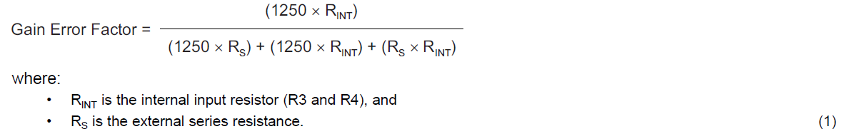
Is the calculation result when RINT is 1.3k-2kohm in the following formula usable?

If No, what will happen?

Currently the value of Rint is less than 10ohm.

I appreciate if you provide some information regarding it.

Let me know if you have any question.

Thank you for your cooperation.

Best regards,
Higa

  • Daisuke,

    The answer is both yes and no. The equations in section 7.4.1 are applicable, and there is even a simplified expression for the INA213:

    However, these equations examine only the ideal scenario where the internal resistance is at the outlined value discussed in the datasheet section. The problem here is that you also need to take into consideration the potential tolerance in the internal resistances:

    This is why we advocate the use of small resistances, as <10Ω's will have minimal bearings on all of these possibilities inside of this tolerance. Using a resistor value as large as 1k will introduce significant error into the measurement as even after you plan the operating point using this provided equation, the value of Rint inside this equation will swing by this tolerance. 

    If the customer needs to use this type of topology, I would recommend looking at a device such as the INA186, which has a capacitively coupled front end, and current limiting resistors have less of an effect on the gain error. Check out this app note for additional information. 

  • Hi Andrews-san

    Thank you for your prompt reply.

    I have some additional questions.

    Is it correct to understand that ± 30% is the standard deviation of ± 1σ? Or is it the maximum and minimum value?

    Does it also includes variation due to temperature?

    Best regards,

    Higa

  • Hi Daisuke,

    I think that 30% is the maximum deviation.

    Don't forget that the internal resistances can show a temperature coefficient which might considerably differ from the temperature coefficient your external protection and filtering resistors. As long as the external resistors are below 10R the effect of internal temperature coefficient would vanish because of pefect internal matching, in the same way as the internal +/-30% manufacturing tolerances will vanish.

    Kai 

  • Daisuke,

    Kai is correct on all counts here. 

    The 30% listed is the maximum deviation in these resistors. 

    Regarding the temperature coefficients of the internal gain network, I've never looked "under the hood" to fully understand this on a transistor level, but I would speculate that the temperature coefficient of this gain network is correlated at least in part to the gain drift of the device, which is a worst case 10ppm. As Kai points out, keeping the external resistors at a value <10Ω will be far more effective in error mitigation here, as the resistors internally are trimmed to each other, which is how the device reaches the values of datasheet spec. 

  • Hi Kai-san Andrews-san

    Thank you for your kind support.

    I would like to present the information from you to my customers.

    Best regards,

    Higa