This thread has been locked.

If you have a related question, please click the "Ask a related question" button in the top right corner. The newly created question will be automatically linked to this question.

OPA462: HV power supply from +/-5V or +/-12V

Part Number: OPA462
Other Parts Discussed in Thread: OPA455, OPA140

Dear E2E Support,

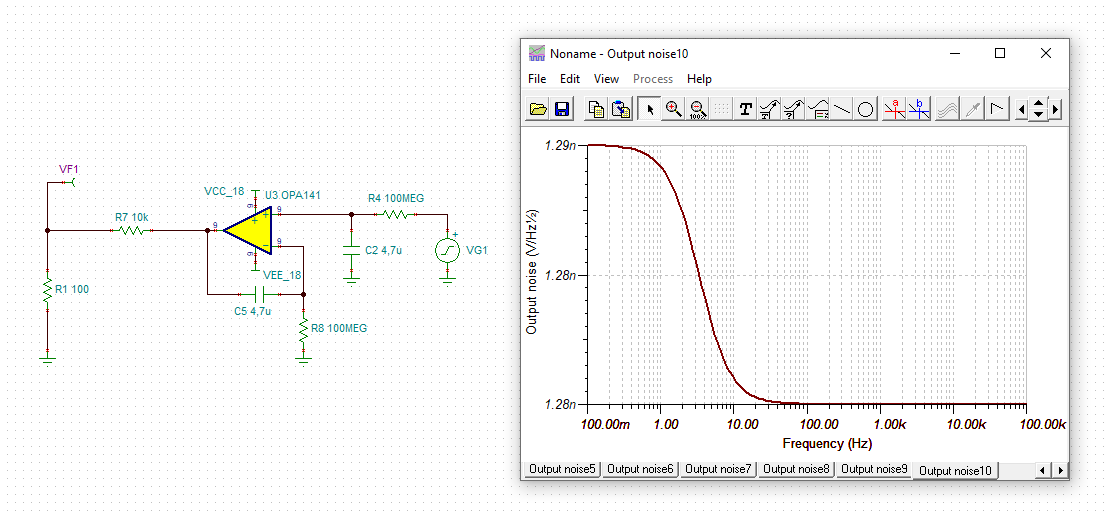
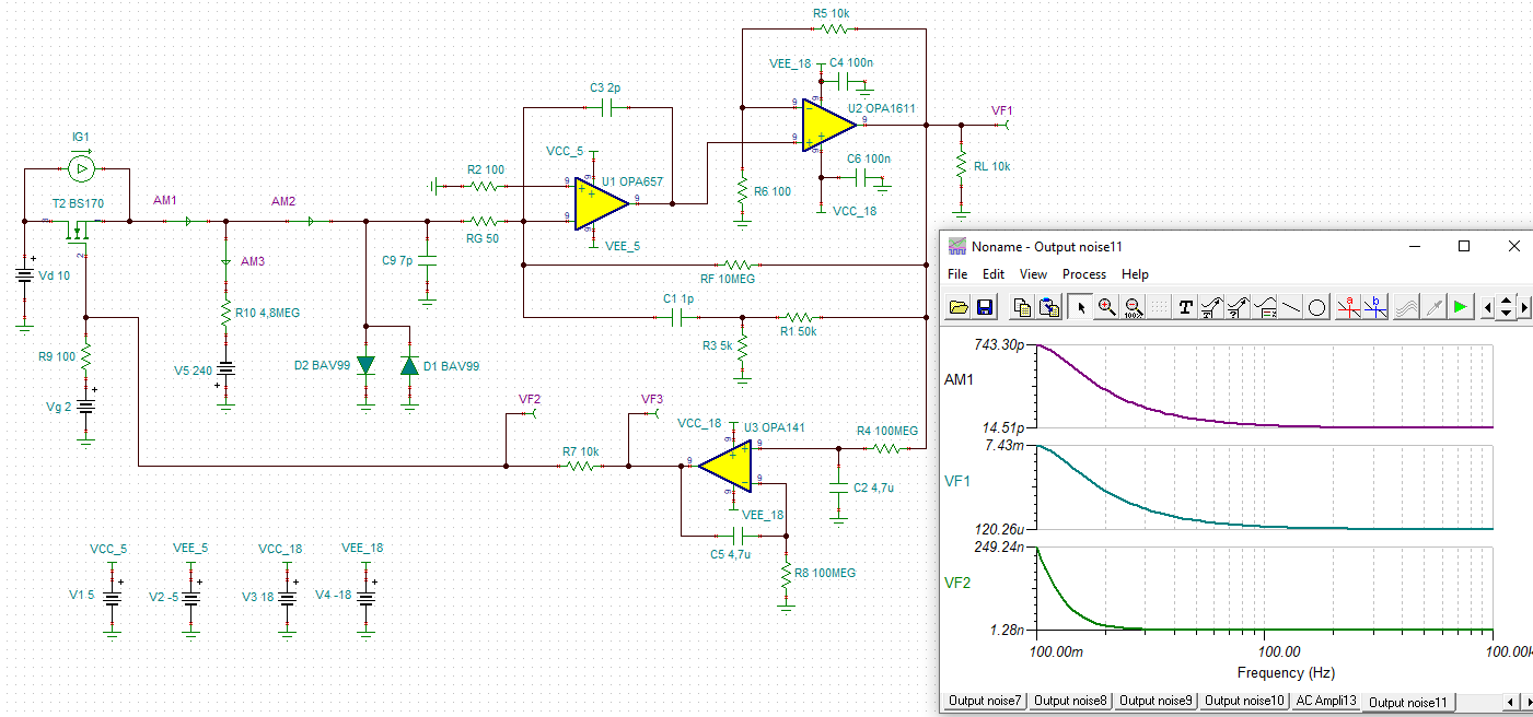
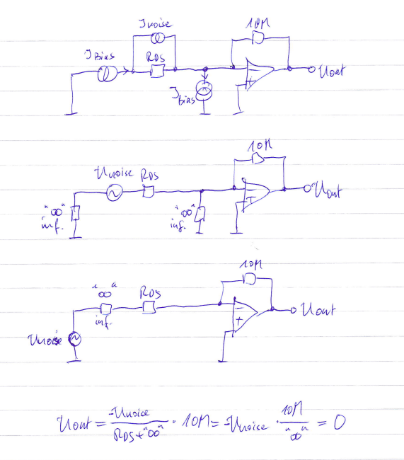
in my application, I need to power OPA462 with +/-90V starting from a DC +/-5V or +/-12V.  Could you please suggest me a low-noise solution ?

Thank you for your help and support.

Best,

Alberto

  • Buon Natale Alberto :-)

    Has it to do with this thread?

    Kai

  • Dear Kai,

    Merry Christmas and Happy New Year to you !

    Somehow, the answer to your question is yes-and-no. I need to test my MOS devices at relatively high-voltage, so using the OPA462, or the newer OPA455

    seems to me a viable solutions. Making a Howland pump without the INA means roaming between resistors to find the best matching. I can think of better ways to have fun... However, I was wondering if the OPA462 (or 455) could be used in the input current suppressor you suggest me in a previous post.

    Your circuit was designed around an OPA140/1, so working between +/-12V. By using the HV OPAs, I could work at nearly +/-100V, an order of magnitude better. In term of noise, that means I could use a resistor ten time higher to suppress the same current at the TIA input. However, the HV OPAs do not have FET inputs and the output noise is quite high. Maybe, could a composite amplifier (OPA140 in input followed by OPA462) do the job?

    Then, should all that stuff work, how can I power the HV OPAs...?

    Thank you for your opinion and support.

    Best wishes !

    Alberto

  • Hi Alberto,

    what is the resistance of your MOS structures when being biased?

    Kai

  • Dear Kai,

    we study the noise current of our MOS transistor, by connecting the source at the TIA input. Drain and gate are biased such to set the transistor in different regions (linear, saturation, subthreshold).

    The DS channel resistance span the range from few ohms to 100k. The Ids varies in the interval from few tens of nA to 100 uA.

    Concerning the current suppressor, it should be able to 'sink' up to 100uA from the TIA input. With a +/-10V supply OPAMP, like the OPA140/1, that means using a 100k resistor.

    Unfortunately, the 100kohm  current noise disrupt our TIA noise floor. Working at +/-100V, your current suppressor could work with a 1M, a value high enough to live with.

    By the way, I guess you are also thinking at the voltage compliance of a Howland current pump based on HV-OPA, like 462. I am aware that with a Howland pump based on OPA462

    I could be able to inject current only to a few kohm load referred to ground. Well, that would not cover all my needs, however could be useful to test the low-to-medium channel resistance range.

    Again and again, thank you so much for your time.

    Best wishes,

    Alberto

  • Hi Alberto,

    Thanks for your post. The engineer responsible for this particular device is on Holiday, please accept our delayed reply. 

  • Hi Alberto,

    I have combined the MOS-Transistor with the TIA and found some interesting results.

    On the left you'll find the MOS-Transistor T1. It's slightly turned-on due to the applied gate source voltage of 3.0V and a current of 6.666245µA flows from drain to source due to the applied drain sorce voltage of about 4V. Is this the way how you bias your MOS-transistors?

    Current sink "IS1" plays the role of bias current "subtractor" and the DC servo arround U3 brings the DC net current flowing into the TIA input down to zero finally (less the input bias current of U1):

    "IG1" shall imitate the noise current. A 100nA sine gives a signal of 1V at the output of TIA:

    alberto_opa657_12.TSC

    It's rather tricky to bias the MOS-transistor this way, because slight changes of gate source voltage or drain source voltage would make the drain source current drift away. So one would want to bias the MOS-transistor by stabilizing the drain source current by the help of a constant current source:

    Unfortunately, the output signal of TIA becomes zero then:

    alberto_opa657_13.TSC

    So you cannot bias the MOS-transistor by the help of a constant current source when connecting the MOS-transistor to a TIA.

    Another interesting result is that the drain source resistance of MOS-transistor itself seems to play a considerable role in the noise of TIA.

    What do you think?

    Kai

  • Dear Kai,

    you described (very) correctly my set-up. That's exactly what I do to measure MOS noise.

    It is a common practice to bias the MOS with a current source, in order to avoid the runaway you have pointed out.

    Please see    and   just as examples of MOS biasing when using TIA to measure noise.

    The 'noise zeroing effect' you have obtained in your simulation is, in my opinion, due to the fact the 'bias' current generator and the 'noise' current generator does not sum up RMS, as they would. Instead, the 'bias' generator overrides the 'noise'. In order to simulate noise in TINA, specific generators/macrosFinding Tina Noise Sources.pdf should be used. See, for istance this TINA short note. However, simulating noise could be very frustrating: the experimental setup is very difficult to reproduce. 1/f noise has to be measured !

    As you pointed out, the Rds is one of the source of noise in the MOS channel. By changing Vgs and the Vds bias, Rds does change and so does the noise. We do explore the noise by varying the bias in the way you reported in your simulation.

    The bottom line is: biasing the MOS with a current generator does not cancel out the noise at the TIA input. What you see is due to the way TINA handles current generators. You can model noise source, however you have to use specific macros.

    I noticed you 'upgraded' R7 to 100M. That's great for noise, but then you can only 'suppress' a very small Ids current. That's why I am considering to set R7 at 1M and use in the servo the OPA462, with its extended supply range of +/-90V.

    Do you think is a viable solution ?

    Thank you so much (again&again) for your time and interest in my application.

    My best wishes of a Wonderful New Year ! If we cannot silence noise, we can at least measure it !

    Alberto

  • Hi Alberto,

    a happy New Year to you too!

    What do you think about the following scheme?

    In a first step you set the drain source voltage "Vd" of your MOS-transistor (T2), the expected gate source voltage "Vg" and the drain source current "IS1" or - more concretely spoken - its "subtractor current" of the same height. Then, the DC servo around U3 fine tunes the gate source voltage of MOS-transistor until the drain source current equals the subtractor current "IS1" (less the input bias current of U1) :-)

    alberto_opa657_14.TSC

    R4 and R8 can be decreased to speed up the settling time, of course. But this will increase the corner frequency of DC servo high pass filtering:

    And, finally, the step response:

    By the way, because of the presence of RG the transimpedance isn't exactly 140dB.

    Kai

  • Dear Kai,

    your idea to put the MOS itself in the servo loop is very interesting. I have only a concern: driving the MOS gate with an OPAMP will inject its 1/f noise into the DUT. In sych kind of tests, the gate voltage is supplied by a lab-grade low-noise SMU (typically made by Keysight or Keithley),  filtered by a low-pass RC. Please, see slide 15 of this presentation Checklist_Successfull_Noise_Meas_and_Modeling.pdf .

    Moreover, in your solution, I would need a 'programmable current subtractor', in order to cancel the variable Ids bias currents at the input of the TIA. A Howland pump current would do the job, but it also adds extra noise, which is not accounted for in your simulation. Moreover, with your scheme, you do not have anymore the full control of Vgs, due to the fine tuning performed by the servo. That means, you do not know anymore the exact working point of the MOS in the (Ids,Vds, Vgs) plane. In noise measurements, you want to study the 1/f noise along the (Id, Vds) loadline and the (Id, Vgs) trans-characteristic. 

    It could be better, I guess, to bias the MOS drain directly with a current source and let the servo 'cancels out' the bias current at the TIA input. It seems to me an easier strategy to follow, which also gives more control to the researcher. The less we interact with the DUT, the better are the results...

    Please, let me know your opinion/comments.

    Thank you so much for your help!

    Best wishes,

    Alberto

  • Hi Alberto,

    well, the whole matter is very very complex :-)

    The DC servo itself works as a low-pass filter, heavily decreasing the noise coming from U2:

    And the noise generated by the DC servo itself is ultra low:

    alberto_dc_servo.TSC

    The bias current subtractor could be made with a high voltage source in combination with a high ohmic resistance. Then the additional noise contribution is negligible, as discussed earlier:

    alberto_opa657_15.TSC

    Alberto, I don't know whether this scheme with the DC servo fine tuning the gate source voltage of MOS-transistor is a viable solution for your application. It's only an idea. The advantage is that the gate source voltage is rather low, doesn't change very much for a certain operation point and can easily be tuned by a low voltage DC servo. So you wouldn't need to use a high voltage Howland current pump or any other high voltage active amplifier.

    At the end of this post, I have a question. Is the following analysis correct? The "lying 8" means "infinitely". The idea behind is that the source impedance of an ideal constant current source is infinitely high:

    I'm looking forward to your reply :-)

    Kai

  • Dear Kai,

    the whole matter is, indeed, quite complex !

    I will definitely test your solution. I am already using your 'current suppressor' (it works great!), so it is very easy for me to close the loop at the MOS gate, instead of the TIA input.

    I have seen your hand calculation. From your analysis, it seems the noise contribution of the two Ibias generators cancel out. While this is true for the average current, their noise sum up RMS, as they are independent noise sources. Beside that, your are right by saying the Vnoise has a Gain -> 0V/V if Ibias is 'ideal' (R->'lying 8'). Unfortunately, this is never the case, so we have to account for a noise gain in real life.

    It should also be noted that noise from the Ibias increases the overall MOS noise and it could be subtracted later in order to obtain the real value.

    I am also very eager to test your 'current suppressor' scheme augmented with a HV OpAmp, like OPA462. I was thinking at a 'composite servo', adding at your original scheme a HV driver based on the 462 or equivalent. There are many possible variants to explore...

    Thank you so much for your opinions. It is a true pleasure to exchange ideas with you!

    Best,

    Alberto