This thread has been locked.

If you have a related question, please click the "Ask a related question" button in the top right corner. The newly created question will be automatically linked to this question.

INA285: output noise

Part Number: INA285
Other Parts Discussed in Thread: INA185, INA190, INA282

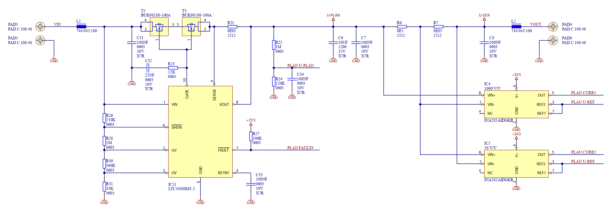
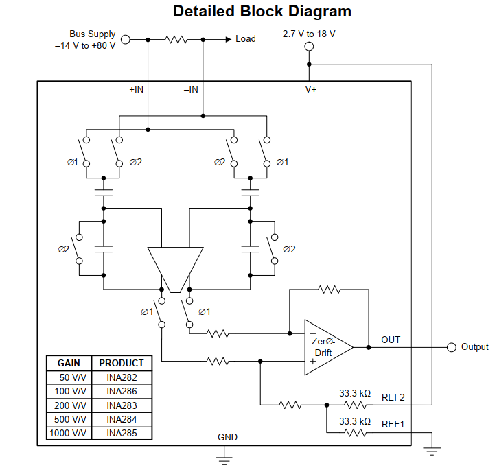
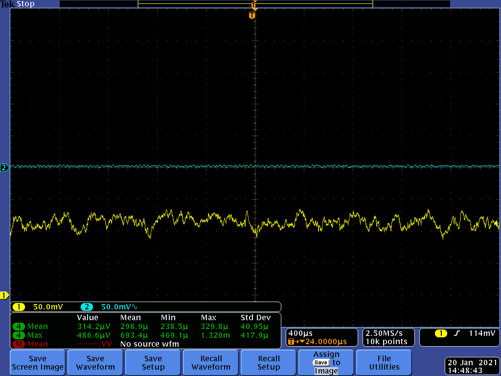
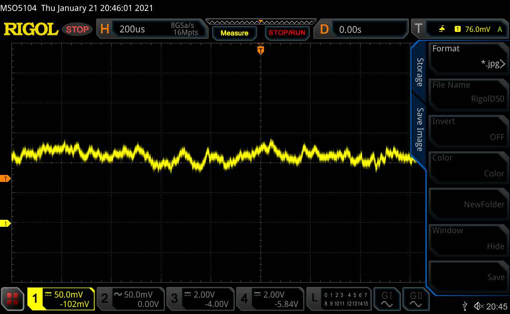
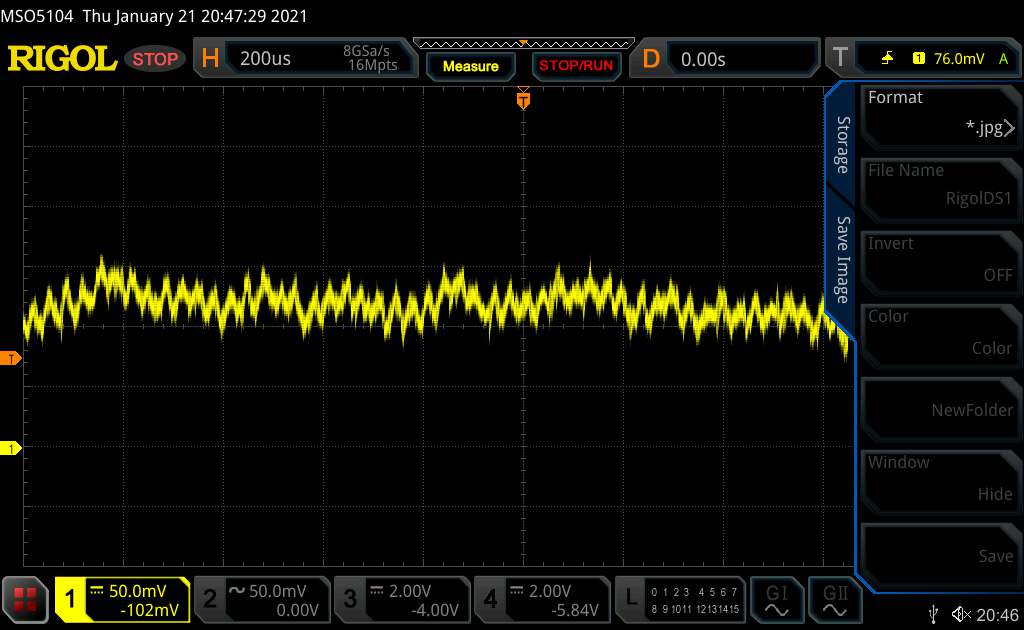
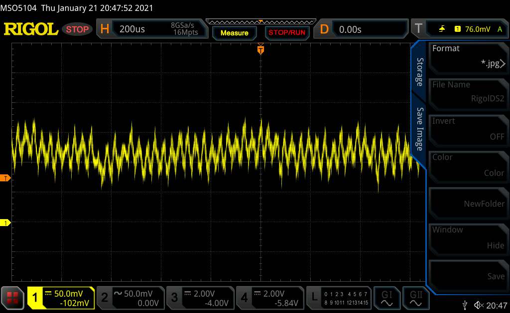
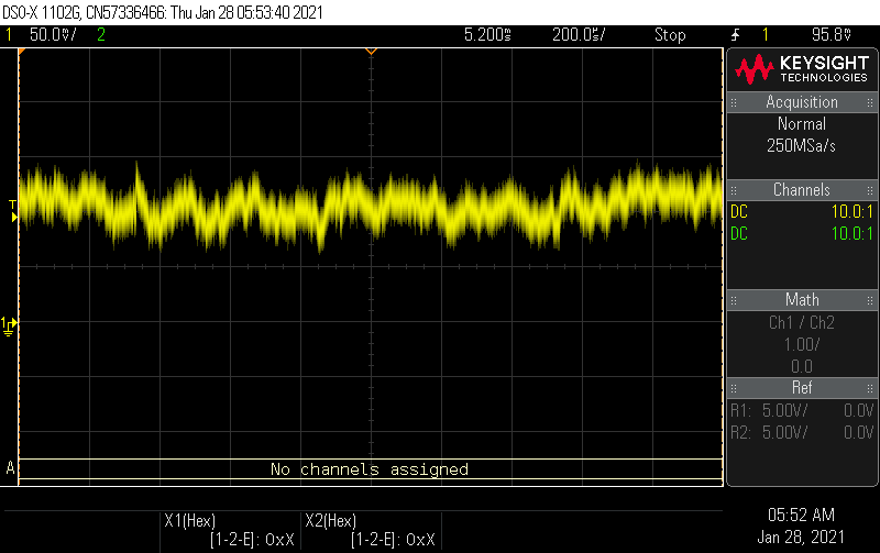
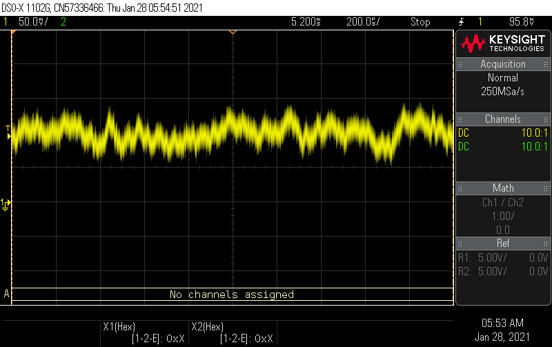
I'm using INA285 for sensing current in the range of 1uA. The chip is supplied with 3.3V. Current will be sensed on the high side of an additional supply. If that additional supply is below 3.3V the output of INA is constant. But if additional supply is increased above 3.3V an additional noise of about 50mV is on the output.

3.3V supply is blocked by 600 ohm bead and a 100n bypass capacitor.

How can I improve the output signal

Best regards,

Gottfried

  • Hi Gottfried,

    a schematic would be helpful :-)

    Kai

  • Gottfried, 

    A schematic would indeed help confirm what's going on. When you say 50mV of "noise," is the output still roughly stable, just 50mV off the expected value, or is there actually 50mVpp of noise centered on the correct value? Either of these conditions could be explained by the graph below, but what's most likely occurring here is that additional offset is being generated at the shunt due to increased input bias current. Can you share the following:

    - What size shunt are you using?

    - What magnitude of current are you measuring?

    - What is the voltage magnitude of the signal measured directly at the pins of the INA185 (not across the shunt), and what is the corresponding output voltage?

    In current shunt amplifiers, when the the common mode of the load line exceeds the magnitude of the supply voltage, the device switches internally to a different input network that is capable of level shifting the higher voltage being measured. This comes with the tradeoff of increased input bias currents at the inputs, of which the current into IN- will flow over the shunt resistor and create an additional input offset voltage. This data is shown in figure 7 of the datasheet:

    It's a tough curve to interpolate, but you can see at 3.3V, you are operating right on the step of the curve such that when your reach the condition you're describing where the voltage of your load line becomes >Vs, you are adding 25-30uA of current through the shunt, and therefore an additional 30uA*RShunt in offset voltage to the input pins of the device. 

  • Dear Kai, Carolus,

    thank you for replay. With noise I mean that the average value is nearly constant, but there is an additional 50mVpp value on the output signal.

    Here you can see the schematic.

    PLAN.U-REF is connected to GND. Shunt for meassuring current in uA range is 0.5 Ohm.

    On first side of datasheet there is an internal schematic with some switches. Can we conclude that the bias current is not constant due to switching cycles?

    Best regards,

    Gottfried

  • Gottfried,

    The images you shared did not come through. Images often break if you copy paste them into the forum. Could you re-upload them using the attach file tool I've highlighted? 

  • OK, here is the part of the schematic:

    As I wrote last time, I think that the switches which shown in the block diagram on the first page of the data sheet will influence the measurement.

    Best regards,

    Gottfried

  • Gottfried,

    The bias curves are not affected by the switching input network with enough magnitude that it would cause this much error on the output. Working backward from your output, a 50mVpp (+/-25mV) signal indicates that you are seeing roughly a fluctuating +/-50uA on the measurement line (25mV/1000/500mΩ) of the input. This is the only condition that changes as you reach the condition of VCM > Vs. Can you probe the output voltage with an oscilloscope to see the noise here, corresponding with the input waveform of the shunt voltage?

    The other explanation is that it could be error in the system. Now that I have a better picture of what is happening here, the other major issue here is the magnitude of the current you are trying to measure against the bias currents and offset voltage of the device. Here is a full scale error plot of your design:

    Examining the curve, between the offset of the device, bias currents, PSRR, etc., your expected worst case error in this range is pretty large.

    The other thing I noticed is you do not have bypass capacitors present on the supply pins of either device. A clean supply is recommended as well, and may be exacerbating the issue.

    Have you looked at INA190? This is the device we typically recommend for measuring uA's as it has bias currents in the nanoamps. They are also relatively constant in the region you are looking to operate. 

  • Dear Carolus,

    In the meantime I have swapped the position of the two amplifiers and their measuring resistors. In the diagram you can see output voltage of INA285 which is the yellow line and signal U-Ser which is the blue line. I'm sorry but I have no equipment to measure the voltage drop on shunt in differential mode and in microvolts. At this measurement there is no load current through the shunt.

    On Ref1/Ref2 I added a voltage of 100mV to prevent the output from running into the limit (Swing to GND). In our circuit we can meassure and compensate any offset value.

    Puting a filter with Murata BLM15AX601SN1D  (600 Ohm @100MHz) between 3V3 and V+ and 100nF between V+ and GND pin has no observable influence. We are using a power GND pair.

    Best regards,

    Gottfried

  • Gottfried, 

    Is it possible in your current setup to place a common mode voltage on each input pin of the device well above the sliding curve, something like >12V? 12V on each pin would bias the common mode of the device to a steady ~22uA while maintaining the VSENSE = 0V condition you are specifying in your current test. This would allow us to verify that is is indeed the bias currents at this level causing the noise on the line. 

  • Dear Carolus,

    with higher common mode voltage (U-PLAN) the shape of the output signal changes

    U-PLAN = 5V

    U-PLAN = 20V

    U-PLAN = 30V

    I have carried out a test with another PCB. Only INA285 and the 0.5 Ohm resistor were mounted. I also used different power supplies. It shows exactly the same behaviour.

    Best regards,

    Gottfried

  • Gottfried, 

    I did some digging, and found that the switching nature of the input cycle is 200kHz for this family of devices. From the waveforms shown here, the nature of the frequency of the distortion looks to be around 30kHz. There is no 30kHz switching w/f internal to the INA185, so I am at a loss as to what is causing this without also being able to see in the input signal.

    As I mentioned in an earlier post, I still believe you will have better results with the INA190, and strongly recommend you look at this device for signals this small. I understand you are performing a calibration here, but even this is no guarantee of performance with signals this small on this device. I took the liberty of generating one last error curve. Notice the zeroed calibrated curves at a room temperature of 25C, and the bearing a 1C difference makes in the error from the calibration point:

  • Hi Gottfried,

    this could be an aliasing issue. Can you decrease the horizontal deflection time?

    Kai

  • Dear Kai, Carolus,

    I think, that I can exclude aliasing. The internal switching frequency of the measured IC should be about 240kHz.

    Currently, the INA190 would certainly be the better choice, but we are thinking about increasing the CM voltage up to 48V. This also means a redesign of the existing layout.

    As I have already written, I have also carried out measurements with a printed circuit board where only the INA and the shunt are fitted.One meassurement at the office another at home with different equipment. I can't imagine that this uneven oscillation comes from externally. Since the block diagram of the INA190 looks the same, I am a little worried that this one will show the same behaviour.

    Gottfried

  • Gottfried,

    The image you posted didn't come through. 

    I plan to get this up on the scope here and see if I can recreate this in the morning. 

  • Gottfried,

    I had a chance to look at this a bit on the bench today, and for my setup, while I am seeing amplification of noise, I am not seeing the periodic signal growing worse with Vcm that you are showing. Here is my setup:

    • Vs = 3.3V
    • Vcm = 3.2V, 5.0V, 12.0V, 24.0V
    • VSENSE = 0V
      • I control the inputs by feeding a direct precision voltage for Vcm to both IN+ and IN- to emulate the condition of Vcm while maintaining Vsense = 0V.
    • REF1 = REF2 = 100mV
    • Scope window was set to the parameters you've established, 50mV/div, 200us/div windows. My DSOX1102G tops out sampling at 250MSamps/s for 200us/div.) 
    • I am NOT performing calibration here 

    With this setup, I do see the noise swing on the signal at this level, but on my setup this looks to be much more random noise than a periodic signal. That said, I've reached out to our designers to see if they have any additional input on such a signal. 

    3.2V (for a Vcm < Vs case):

    Vcm = 5.0V:

    Vcm = 12.0V:

    Vcm = 24.0V:

  • Hi Gottfried,

    can you show a photo of your measuring set-up?

    Kai

  • Hallo Kai and Carolus,

    that measurement look the same that one with low voltage which I had posted. Now I have repeated my measurements at my workplace at home and at my company. That about 30kHz distortion comes from the power supply unit I use at home. I cant see that distortion on workeplace in my company. The output signal looks like you posted from very low up to 30V common mode voltage.

    Gottfried

  • Gottfried, 

    I thought this was the issue you were questioning? With the 30kHz signal explained, I honestly believe the remainder of what we are seeing in our combined scope shots is mainly noise. 

    From your schematic, there is no filter installed at the input or output of the device limiting frequencies. This means that the full noise bandwidth is present on the device. Looking at figure 15 of the datasheet and treating the response as a pure brick wall at 10kHz, the RMS noise of the device is calculated to be 10.94uVrms, and multiplying by 6 gives 65.67uVpp at the input, which is gained by a factor of 1000, so your noise floor on the output is about 65.67mVpp. This curve is for the INA282, so I would actually expect the INA285 to be slightly better in terms of noise given that its bandwidth is 2kHz vs 10kHz, but it is also not a true 20dB/dec response from the roll-off, so I would interpolate the noise to be somewhere marginally inside this value. This more than explains the 50mVpp noise fluctuation you are seeing, before taking into account the other factors we've discussed. The only thing I can recommend to counter this is to place a filter either on the input of the device (which may work easily since you are already performing a calibration) or the output and set the cutoff at some small value, such as <1kHz to maximize the gain performance against the noise of the system.