This thread has been locked.

If you have a related question, please click the "Ask a related question" button in the top right corner. The newly created question will be automatically linked to this question.

THS3491: Power FET Drive Circuit

Part Number: THS3491

Hi team,

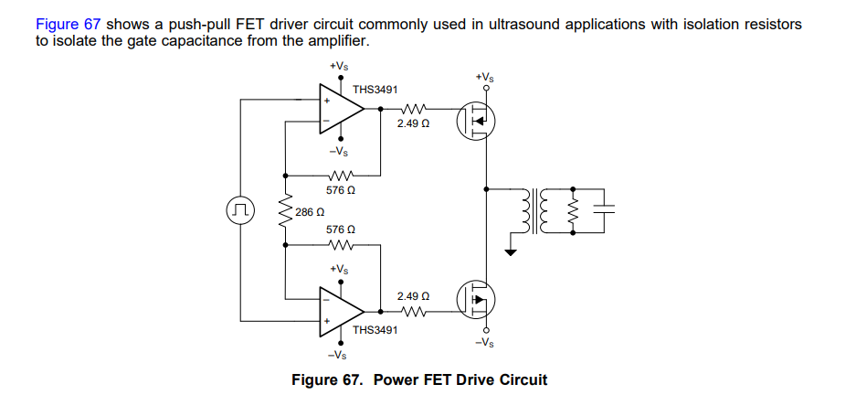
Figure 67 of THS3491 datasheet is shown in the figure below. In the upper part of the figure is N-MOSFET, whose source is connected to the highest potential +VS. Even if the maximum output of ths3491 is +VS and connected to the gate of N-MOSFET through 2.49 Ω resistance, the VGS of N-MOSFET must be less than or equal to 0. The condition for N-MOSFET to turn on is that VGS is greater than a positive threshold voltage. Is N-MOSFET in the figure unable to conduct?

Similarly, the P-MOSFET in the figure also has this problem.

  • Hello Amy,

       The N-Mosfet for this push-pull circuit will be conducting in the positive half of the signal, while the P-MOSFET will be conducting in the negative half of the signal. There will be a region around 0.7V where both FETs will not be conducting due to the internal diodes forward bias. This is where crossover distortion occurs. These FETS have their drain connected to the power supply of the amplifier, not the source, which I believe is where the confusion arises. The source for these FETs are connected to the transformer which has a ground reference. Therefore, the MOSFET will conduct above the VGS threshold specified in the selected FET's datasheet (usually between +/-3 to +/-5V). 

    Thank you,

    Sima 

  • Hi Sima,

    Thank you for your reply. That's what makes sense. In my opinion, the MOSFET symbol in Figure 67 should be modified to avoid confusing other users.

  • Hi Amy,

    I aggree with you. The MOSFET symbols are wrong :-)

    They should be swapped.

    Kai

  • Hello Amy,

      Whoops, that is correct! The diagram shows the sources connected not the drain. Will get that modified, thank you for the catch on this!

    Thank you,

    Sima

  • Hi Sima,

    I use TINA to simulate the figure 67 circuit. The output levels of the two OPA are opposite, that is, one is high level and the other is low level. Therefore, two MOSFETs are on at the same time. I don't know how this circuit works. Is it related to the signal I input?

    Power FET Drive Circuit.TSC

  • Hello Amy,

       I would parallel the amplifiers with a push pull driver this way instead of what the figure shows:

    The top MOSFET turns on above 3.1ishV, while bottom MOSFET will be off. Then for the next half-cycle, the bottom MOSFET will turn on above 3.1ishV, while the top MOSFET will be off. There will be a period where both MOSFETS will be off which causes some of the crossover distortion you see in the middle of Vout's sin wave value transition. Increasing the offset voltage VMID would help minimize this crossover distortion.

    Amy_Power_FET.tsc

    Thank you,

    Sima

  • Hi Sima,

    Thank you very much for all your done, but I see that you have also modified the power supply and MOSFET. I wound like to know whether figure 67 in the THS3491 datasheet can work normally. Because I think since it is shown in the datasheet, there must be a reason for it.

  • Hi Amy,

    I think the circuit from figure 67 is crap :-)

    A push pull stage can be made either with a PMOSFET and a NMOSFET or with two NMOSFETs. In the first case the both gates should be connected together and should be driven by the same signal, or by other words, without any drive signal inversion. This is obviously impossible with this circuit.

    With two NMOSFETs, on the other hand, both gates should be driven by inverted signals but which additionally should toggle between the both supply voltages of MOSFETS. So with two NMOSFETs in the push-pull stage the circuit could indeed work, provided that both outputs of OPAmps can fully swing to the supply voltages of MOSFETs :-)

    Another option is to use a center tapped transformer with the center connected to a positive supply voltage :-)

    Kai