This thread has been locked.
If you have a related question, please click the "Ask a related question" button in the top right corner. The newly created question will be automatically linked to this question.
Hello Team,
Good day.
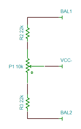
My customer is looking for design parameters for BAL1 and BAL2 pins for the LF411 device. The datasheet has limited information on these pins, can you share any information we can use?
Regards,
Renan
Hello Renan,
The balance pins connect to the input stage resistors that terminate to VCC- pin. Typically an external potentiometer wiper connects to VCC- and the two ends go to BAL1, BAL2.
The LF411 is very old device, we have better modern devices for new applications.
Hello Ronald,
Good day and thank you for this response.
My customer really wanted to use this device and wanted to know further about these pins. Is there a recommended value for the external potentiometer? As well as, is there a correlation or equation that represents the values or trimming of the external potentiometer?
Regards,
Renan
Renan,
I have some LF411 samples in stock. I will measure the internal resistance so I can suggest an external pot value.
Answer in about two days.
Hi Renan,
this appnote recommends a 10k trimmer:
AN-447 Protection Schemes for BI-FET Amplifiers and Switches
Kai
Renan,
A 10k pot does work, but it is too powerful. the op amp output can be forced to VOL or VOH if the pot is turned too close to either end.
Adding 22k resistors to the pot ends helped. With this, the tuning range was +/-6.8mV. Make R2,R3 bigger to reduce the range or make them smaller to increase the tuning range. 12.7k was +/-15.3mV