This thread has been locked.

If you have a related question, please click the "Ask a related question" button in the top right corner. The newly created question will be automatically linked to this question.

INA250: INA250 Propagation Delay for Pulsed Current Input

Part Number: INA250

There is significant Delay between Input Current and Output Voltage. Delay depends on Input Current level.

See the attachment for details.. (if you cannot open file, please give me your e-mail address so that I can send it directly..TI Inquiry INA250 for E2E.pdf)

  • Please post the pdf again and use the "Insert File" button (paper clip) :-)

    Kai

  • Hello 6541046,

    Can you attempt one more time to post the pdf the way kai mentioned above?  If you are still unsuccessful, I will send you a private message with my email contact.

  • Here I upload again the pdf.. Maybe you cannot open it because of our compnay encriptioin..

    If I send it by e-mail, the encription will be unlocked..

    1781.TI Inquiry INA250 for E2E.pdf

  • Yes, it's still impossible for me to open it :-(

    Kai

  • Hello 6541046,

    That is quite a significant delay, which our part should not be exhibiting.  My initial thoughts are that either you do not have the INA250 adequately powered on before the current passes through the shunt, or there is a discrepancy between your current monitor and the current going into the INA250 due to the inductance from long skinny wires/traces.  For the first possible cause, I think monitoring the device supply will be helpful.  For the other possible cause, I would try using shorter, fatter wires. Yet if that is not the issue, it could possibly be that capacitor you have in front of the laser Diode.  How big is that cap and where are you getting your green signal from?  If that is a large cap and it is discharged to a voltage below your laser diode turn-on threshold, it could be pulling alot of current during the charging process from your supply while siphoning much of it away from the path that goes through the INA250.

  • Hello Kai,

    It looks that the uploaded file is encripted due to my company security..

    If you can let me known your e-mail address, I can send it to you directly.. In this case, the file will be decrypted..

    Yonchan 

  • Hello Patrick,


    Thanks for your advice.. I have checked your points :


    1) Device Power Supply : +5V is adequately supplied to VS Terminal of INA250 EVM.
    2) Indcutacne of Wire : For test purpose, I have removed the wire (~30cm each for connecting Laser Anode and Cathode but it is quite thick enough)..
    Instead, a dummy diode (lead type) is connected directly to Laser Driver Module and I have observed no effect on the delay..
    3) The Capator : Capacitance is ~1000uF (Two Capacitors in parellal 470uF//470uF)..
    4) Current Probe : It is located at the High Side of Shunt Resistor of INA250.. Green Signal (=LD Current) is invariant whether it is located at High/Low Side of the Shunt or at Anode/Cathode of Laser..
    5) Charging and Discharging : The Capacitor stores enough charge and discharges during the Laser-On Time.. Power Supply charges the Capacitor (current increasingly flows into the Capacitor to make up the discharge..) I checked the Capacitor volatge maintaining >4.5V during the on-time..

    So I suspect the delay (especitally for Low Current) is coming from INA250 chip itself..
    The Shunt Resistance is only 2mOhm thus when 0.36A current is flowing through the Shunt, the Input Voltage to the amplifier is only 2*0.36=0.72mV..
    Is this normally detected by the amplifier?? 


    Kind Regards
    Yongchan

  • Hello Yongchan,

    Thanks for checking those items for me.  I will try to do some bench tests tomorrow to see if I can duplicate your results and then I will share whatever I find.

  • Hello Yongchan,

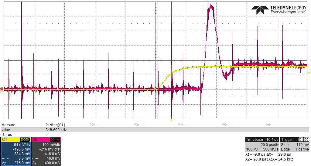
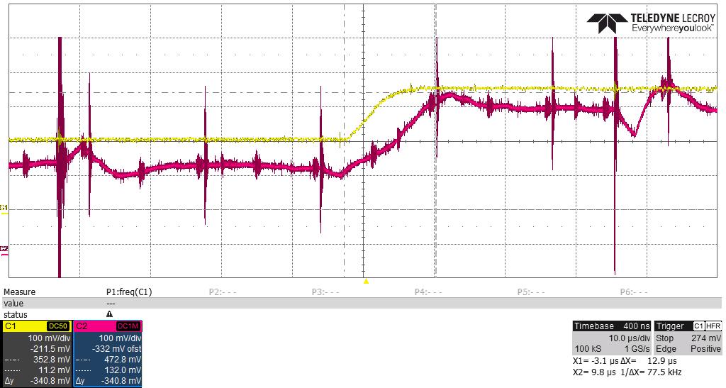
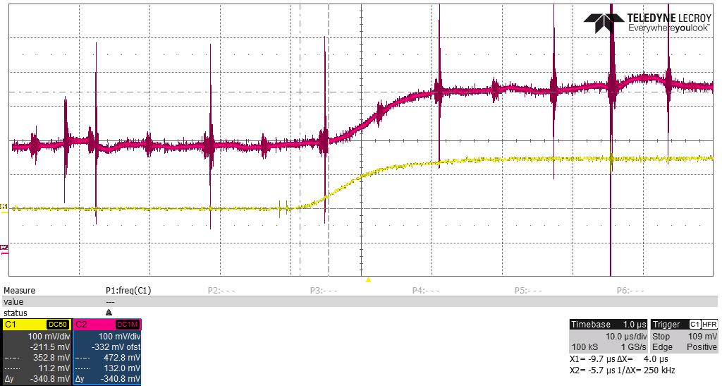
    So I ran some tests today and saw a similar issue.  My delay was only 30us and I used an A2 gain variant, because I did not have any A3s on hand.  After  discussing with a colleague, it seems to be a combination of device offset and having the reference at ground.  The device offset can be both positive and negative.  If it is negative, the offset gets amplified and tries to push the voltage below the ref pin, which is already at ground.  In this particular instance the device is outside of the linear operation and the transition outside of this region can look like a delay.  So there are two ways I saw to resolve this issue.  One was to have your base current high enough to overcome and voltage offset referred to the input, which I suspect is not an option for you.  The other would be to provide some non-zero voltage reference.  Below are some of the measurements I collected.  I apologize for the quality of these measurements. These admittedly look pretty noisy and that is due to the extremely noisy supply to the eload I had to work with and the circuit path not being optimized.  However, I do think these illustrate the proposed fixes will help with the delay issue.

    Yellow = Eload Imonitor, Magenta= INA250 Vout

    Initial Case, Vs=5V, Vref=GND, 0.36A step, transition ~30us

    2nd case, Vs=5V, Vref=GND, 0.5A to 0.86A step, transition instantaneous

    3rd Case, Vs=5V, Vref=300mV , 0.36A step, 4us

  • Hello Patrick,

    Thank you for suggesting a solution with experimental evidence..

    I have just finished a replica test, suppling +0.5V to VREF and finding that the delay is reduced from 76us to 12uS, which clearly solves the issue.. 

    I am pleased with the result and going to send the details of my test by e-mail tomorrow..

    Kind Regards,

    Yongchan