Other Parts Discussed in Thread: TLV4111, TLV4110
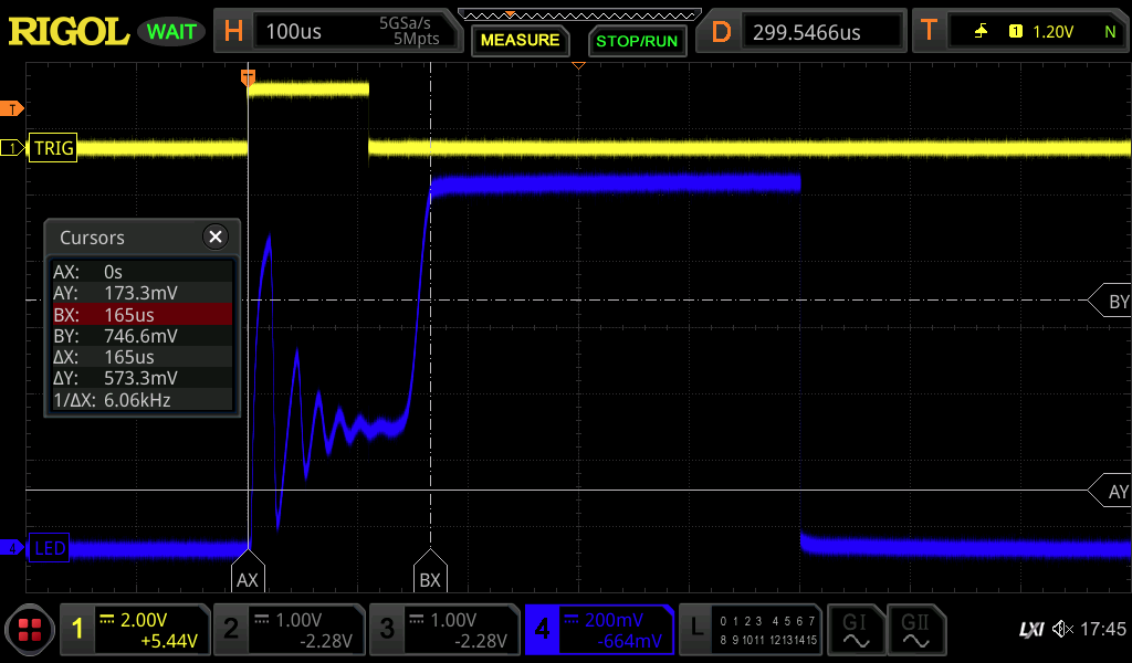
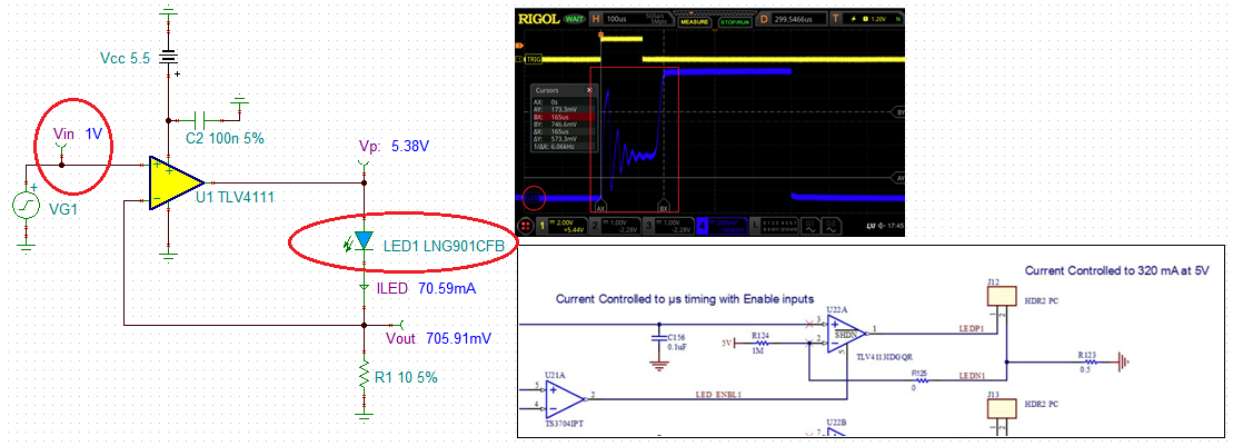
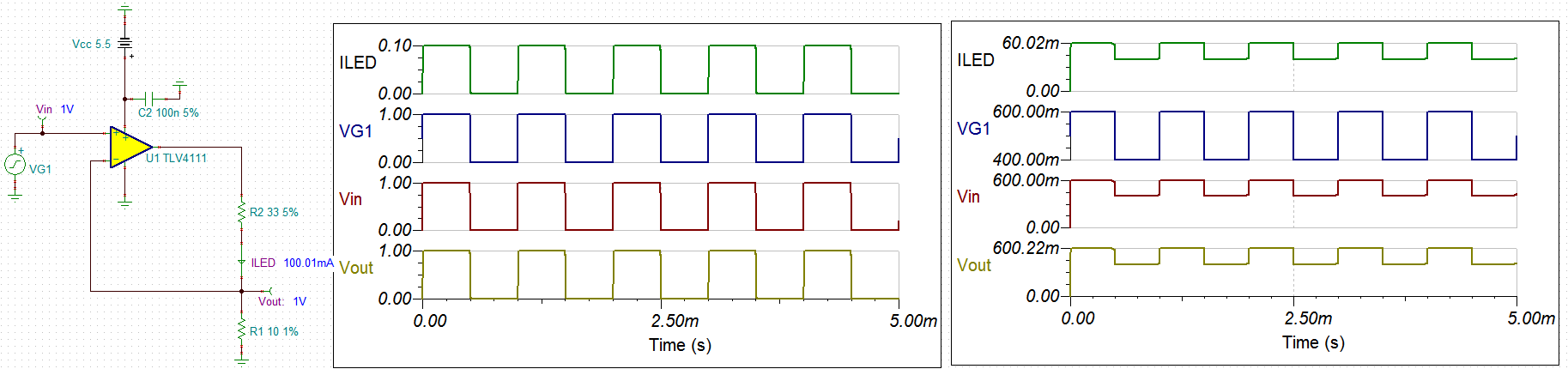
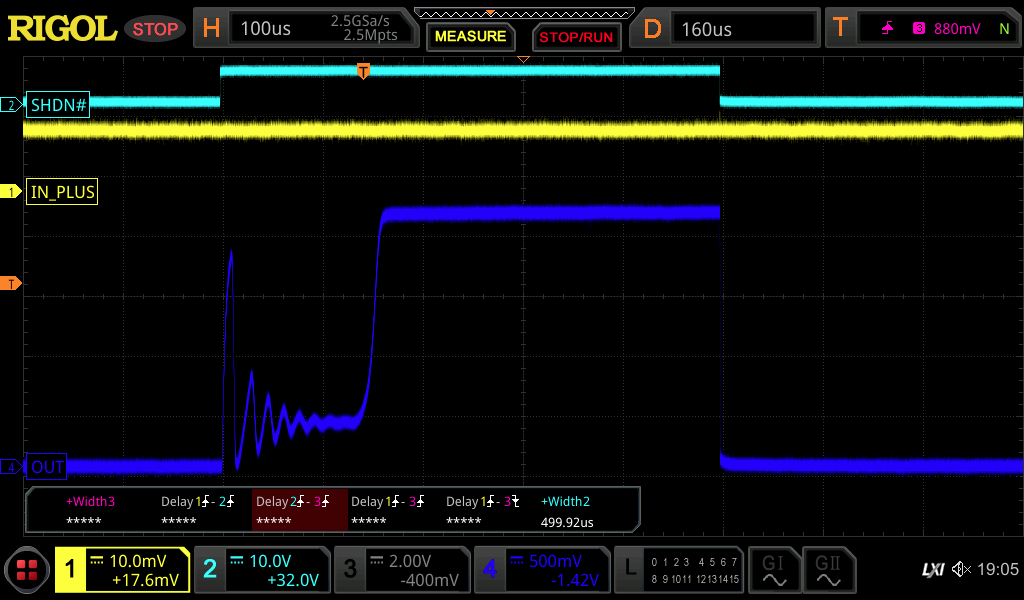
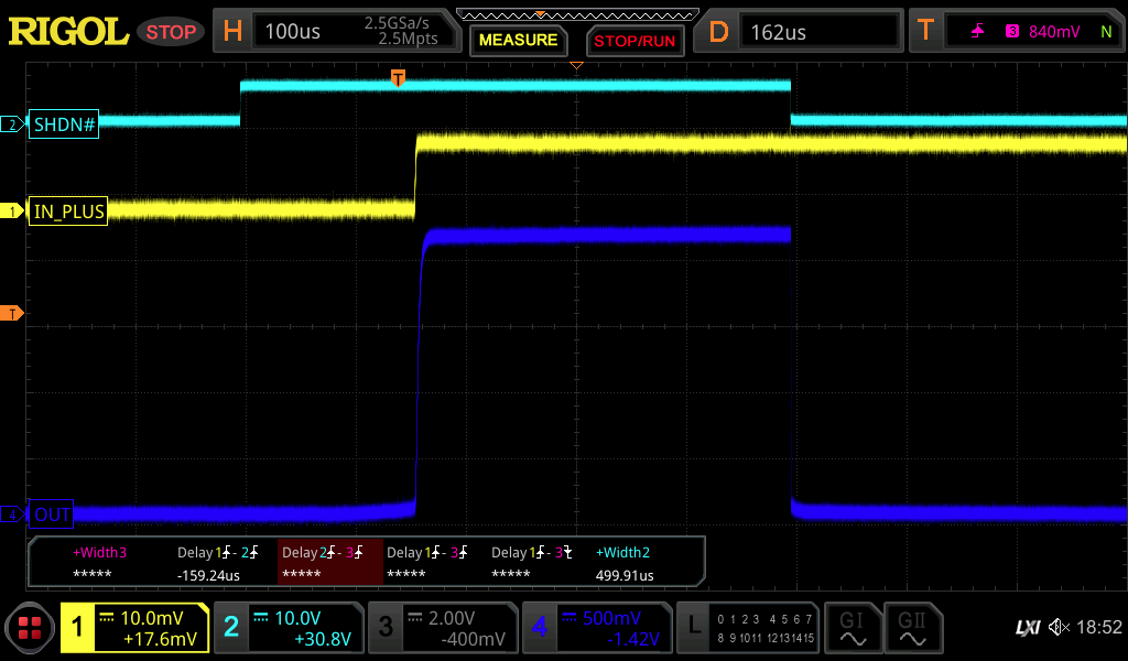
When driving a 10 Ohm resistor on the output of the TLV4113 with a 1V output for 100 mA current. The input of the OpAmp was stable while the SHDN# was pulled high.
We note about 200µs of leading oscillation before the output stabilizes. At lower voltages, the oscillation is weaker, but there's still a 200µs period before stabilizing.