This thread has been locked.

If you have a related question, please click the "Ask a related question" button in the top right corner. The newly created question will be automatically linked to this question.

INA125: What is the recommended way for balancing or 'Zeroing' inputs from a strain-gauge Wheatstone bridge into or through an INA125 or similar?

Part Number: INA125
Other Parts Discussed in Thread: XTR106, INA333

I'm building a very sensitive load cell (~100 µN) using strain gauges in a full Wheatstone bridge configuration (4 strain gauges).
The Wheatstone is excited with 5V and the sense nodes are connected to the inputs of the INA125 powered with a single 15V supply.
The load cell is very sensitive so even before applying a load, the output of the bridge is unbalanced and presents -5 mV input into the INA, which (because the input is negative) outputs 0 V.
As I apply a load, the balance of the load cell shifts and the input into the INA eventually reaches 0 and then grows to 5 mV.
The problem with this setup is that the load cell (and amplifier) have a large dead zone (-5 to 0 mV) before I start getting an output signal.

Is there a way to modify the INA circuit to implement some input offset so that it compensates for the load cell's offset? 
Would adding a trimpot between pin 10 and pin 11 have such an effect?

Alternatively, is there a similar amplifier that may help me solve this?

Thank you for your consideration.

  • Hi Rodrigo,

    ~100uN is approx. 100mg of weight or force. It is like a micro balance scale. Anyway, can you try our INA821INA828INA819  or INA818 Instrumentation amplifiers (IA), which are better to handle this level of sensitivity. 

    Enclosed is a link about IA selections.

    https://e2e.ti.com/support/amplifiers/f/14/t/818894

    Is there a way to modify the INA circuit to implement some input offset so that it compensates for the load cell's offset? 

    Assume that this is micro balance application, input offset compensation button is equivalent to TARE button on a  weight scale. Alternatively, you can use software to remove the offset voltage at the output. 

    I do not like to add trimpot for this level of sensitive measurement. We can simulate the IA circuit, if you provide us with wheatstone bridge parameters and gains. 

    If you have additional questions, please let us know. 

    Best,

    Raymond

  • Hi Raymond, 

    Thank you for your prompt and insightful response. I've reviewed the references you pointed to about INAs and have learned a great deal that will help me reduce the noise of my design. The other amplifiers you suggest look very interesting too. However, I do like that the INA 125 has a built-in reference. Do you still recommend switching to the other INAs?

    Slight clarification, 100µN is ~10mg so we need an extra 10X to get there.

    The larger context of my design is to make a load cell to test the mechanical performance of some micro-fibers across many cycles. Therefore I need considerable stability. 

    The main issue I'm having with the offset is that in the default state, for some reason my load cell outputs a Vd of ~11.0 mV with a common mode of ~2.5V. So it is unbalanced, to begin with. After I apply the 0.7g load (I know this is beyond the target scale but it is easier to work with for now), the Vd changes to ~10.9 mV.   I estimate the sensitivity of the load cell is 0.014 mV/mN  
    Ideally, I would like to set the INA gain to ~1800 to get a 2.5V output swing with a 100µN change into an ADC. However, since the initial Vd is already 11.0 mV with a gain of 1800 this becomes ~19V which saturates the output of the INA (driven with 15V).   I can't tare this or zero this with software

    I'm working on building another load cell that will hopefully be balanced properly, but in any case, given the high-gain requirement, and potential initial un-balance, If we had to add trimpots, where would it be a good place?  

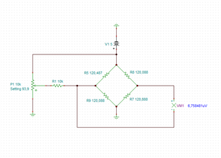
    I would very much appreciate a simulation of the IA! I'm currently using a full-bridge Wheaton where every strain gauge has a default value of 120Ω. Following are values I have back-calculated (using a solver) of the 4 resistors in the static and loaded case, and the change I see in each resistor between base and loaded. Let me know if you need any other info.

    base: 120.487 120.088 120.888 120.088 
    test: 120.335 120.335 120.735 120.335 
    change: 0.9987 1.0020 0.9987 1.0020

    I am considering switching to other strain gauges with 350 Ω of 1000 Ω initial resistance with the goal of reducing the current and heating effect I see with the 120 Ω load cells.  Do you have insights as to how this would affect the stability of the system? 

    I started this project in September thinking it was a quick and dirty PCB and I have now peeled through many unexpected layers of complexity.
    I'm extremely grateful for your input and support in driving this to its final conclusion. 

  • Hi Rodrigo,

    Q: I can't tare this or zero this with software.

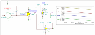
    Since you are using single rail of 15V, you need to elevate INA125's Vref pin, namely IAref in pin5 to approx. mid rail of 7.5V. You signal is likely very small, may be 5V may be adequate, see the attached plot. This will make linear output vs. input due to input common mode vs. output voltage. 

    If you use dual supply rail, IAref or pin5 can be configured to ground. I would recommend that you use +/-5V or so to operate INA125, if you prefer (you may need a different type of sensor). IAref voltage in INA125 has to be stable,  low impedance voltage reference, see Application information on p.10 of the INA125 datasheet. 

    INA125 is nice, because all necessary building blocks are integrated in the high performance IC. The nominal bias current is 10nA (25nA max in INA125P, U package). If you have a sensor that is able to  source the sensing voltage and current, I would use this. If you need higher input sensitivity, lower noise, lower offset and drift over temperature, you do have other options. 

     Q: potential initial un-balance, If we had to add trimpots, where would it be a good place?  

    If I understood your requirements correctly, you want null out the initial error in the wheatstone bridge with 0.00mg. You may perform this task at your input bridge sensor. Of you can calibrate out your offset or imbalanced input errors at the INA125's output (two point calibration between 0.00mg and 10.00mg).

    Enclosed is a Tina INA125 pseudo simulation example that it may help you to understand the performance of IC better. I do not have your sensor and gain parameters, so you need to reconfigure these settings. If you need help, please let me know. 

    /cfs-file/__key/communityserver-discussions-components-files/14/INA125-Bridge_5F00_Amp-Strain-Gauge-02032021.TSC

    Q: I am considering switching to other strain gauges with 350 Ω of 1000 Ω initial resistance with the goal of reducing the current and heating effect I see with the 120 Ω load cells.  Do you have insights as to how this would affect the stability of the system? 

    I think that you may need to use higher resistance wheatstone bridge sensor, since the Voltage reference is able to source approx. 5mA or so. As you indicated, it may reduce the self heating at the sensor somewhat. If you use 120Ohm load cell, the voltage reference may not have enough current to drive it. 

    Are you talking about thermal stability in the sensor or INA125? INA125's thermal stability is fairly good, 2uV/C max. In addition, the instrument is likely operated indoor at ambient temperature, so it should not be a concern. Electronic stability should not be an issue as long as the INA125 is not driving capacitive load at its output. 

    When you select a weight bridge sensor, you need to select one with full scale range as close to your 10.00mg range. This way you have enough sensing resolution vs. force in dynamic range. 

    If you have other questions, please let us know. 

    I forgot to mention that we have LM7705 low-noise negative bias generator (switched capacitor voltage inverter). If you input 3-5.5Vdc at the regulator's input, it will generate -0.232V regulator output voltage. If INA125 is negative biased at its V- rail, your initial offset issue at no load condition may be resolved, and keep IAref =0V or ground. Please check it out with the simulation.  

    Best,

    Raymond

  • Hi Rodrigo,

    Here is our INA Common-Mode Input Range Calculator for Instrumentation Amplifiers. The IA calculator may be very helpful  in part selections and design. 

    https://www.ti.com/tool/INA-CMV-CALC

    Best,

    Raymond

  • Generally, compensating such an offset is done at the bridge, by adding a fixed shunt resistor to one of the two adjacent arms on the same side of the bridge. The resistor type would be ideally selected to match the tempco of the bridge, or you can use two resistors in a ratio to ensure their tempcos yield a null resultant error.

    In small scale production you'd use a multimeter with some connection to the PC and write a little python script that measures the voltage and uses that to compute the resistor selection as well as the connection point (upper vs lower arm of the bridge half). This can also be done by the various Excel plugins available for many voltmeters - then the calculation and resistor selection would be done in the Excel spreadsheet. Make sure to protect the relevant cells so that inadvertent input doesn't corrupt the spreadsheet.

    There are many other options available. INA125 has a built-in excitation voltage reference, and it is a part designed I guess in the 90s? There's a reason for this voltage reference - it is useful mostly only in a very specific application. That is: if you need an analog signal output from your product with a long-term-constant gain and don't have an MCU in your system. I imagine that this was the specific application that part was designed for (I only guess of course), and that a "typical" use case was for built-in transducer signal conditioners, back when integrating an MCU inside the sensor was not typically done due to cost and size constraints.

    If there's an MCU in the system, it may be cheaper to digitize the input, calibrate and otherwise process it in the MCU, then output it as a calibrated analog voltage (using a stand-alone DAC, a PWM output switching between a reference voltage and ground, etc.). But once you're in charge of digitizing the signal, you don't need a precision reference voltage anymore, since you can perform ratiometric measurements: the ADC's reference voltage is scaled from the excitation voltage provided by any low noise voltage regulator, with no particular requirement on absolute excitation voltage accuracy (a couple percent will do just to maintain sufficient transduction gain). That way, the arbitrary units the ADC outputs will correspond to a given change in the resistance of the bridge's arms, independently of excitation voltage - only the noise will increase as the excitation voltage drops (eventually you'll run below the minimum ADC reference voltage of course).

    Other potential options may be as below, and that's just a very small sampling of them, and not all make sense in every application of course:

    • Connect the sensor directly to a high resolution ADC, with no preamplification, and perform taring in software, or using the built-in offset calibration feature of the ADC. You may find out that such an ADC costs in the same ballpark as an INA125 would (likely less), given other precision parts you may need to apply it.
    • Connect the sensor directly to an MCU with a built-in direct low voltage sensor interface (say, an ADC with a selectable inherent conversion gain, acting like a PGA but without an actual PGA).
    • Use an in-amp with a digitally programmable offset.
    • Split the gain into two: first stage gain, then add a current from a digital potentiometer or DAC or even a PWM output into:
      • the summing node of the 2nd gain stage, or
      • the REF input of the 1st-stage in-amp, but make sure to stay within the input-output voltage polygon of the in-amp. Raising the 2nd stage gain helps here, usually at the expense of the effective offset and noise of the 1st stage. Also, the REF input in three-amplifier in-amps needs to be low source impedance to maintain CMRR, unless otherwise specified, or unless you're using an amplifier with true differential output, with suitable output CM range.
    • Connect a digital potentiometer, through a series resistor, to one output of the bridge. This does decrease AC CMRR since there'll be different stray capacitances tied to each side of the differential input, so sometimes it helps to choose a dual potentiometer with a layout that'd allow a fully symmetric application, with the (+) signal traces and components laid out as the geometric mirror image of the (-) signal traces and components. The digital potentiometer can be programmed from a "bit-banging" production jig that uses e.g. an FTDI USB-to-parallel interface, or a stand-alone Arduino running through a serial terminal on the PC, so there's no need for an MCU on-board. Some older digital pots even have up/down/store "button" inputs, so a very simple passive adapter can be used to set the offsets.

    In other words: a lot depends on the application, and the time you have available to develop said solution. My favorite answer to "how do you zero bridge output" is always - don't even do it if it can be avoided. The "classical" bridge - in-amp - filter - buffer - ADC signal chain isn't be best choice for every application. It can be almost always made to perform very well, but it may be costly and inflexible at times. It is a good starting point in exploring the design space, of course.

  • Hi Kuba,

    My favorite answer to "how do you zero bridge output" is always - don't even do it if it can be avoided.

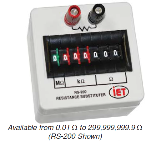
    That is what I am trying to suggest from the previous reply. However, if you want to do it at the bridge side, you may connect one or two of digital decade box below and manual balance the sensing bridge, see the link below. Please make sure that the resistor box is rated for the current application (don't over heat the resistor box). I used similar box in a lab in the past and it works well. 

    As you indicated, once you found the balanced bridge in DC, you can replace the balanced R value with a matching Tempco resistor. You may get a resistor box with microOhm resolution if an application is called out. Your Wheatstone bridge should be in 1 kOhm range or so, 0.1Ohm to 1Ohm/step resolution may be more than adequate. 

    Alternatively, you can measure a voltage across an output of the wheatstone bride, and calculate and insert a matching resistor value and null out the output of a bridge under no load condition.     

    https://www.mouser.com/datasheet/2/194/RS-CS-LS-571.pdf

    If you have additional questions, please let us know. 

    Best,

    Raymond

  • Thank you so much for all the feedback @Raymond and  !

    Through your help I have managed to rework my latest revision of the load-cell amplifier (based on INA125) to give me somewhat functional results, and through your pointers and references I have learned very much about the requirements for this project. What I thought would be a trivial amplifier required considerably more depth. 

    I'm preparing to do a next revision of a board and would appreciate some oversight. Would either of you be available for a short consulting project to oversee the design choices and part selection? I'm particularly interested in 's suggestion to use a modern INAs and a common reference as a work-around to having a very precise one.

    Please message me directly if you are available for a brief advisory opportunity. 

  • Hi Kuba,

    Thanks for your detail write-up about Rodrigo's inquiry. 

    Hi Rodrigo,

    Could you remind me which "zeroing" wheatstone method you would like to implement in your next design? Kuba suggest several, and we have wide selection of modern Instrumentation amplifiers (IAs) as well. The information that I would like to know. 

    a. Are you going to use MCU to calibrate out the IA's offset voltage? Perform 2 point calibration in Vout vs. applied force at transducer. 

    b. Do you want to keep INA125 or use other modern IA parts?

    c. Is the application going to be single supply rail at 15Vdc?

    d. What is excitation reference voltage you are going to use? Is it 5Vref_excitation?

    e. What is Vref voltage at the output of IA application?

    f. What is the Gain configuration for the IA? still Gain=1800. 

    Anyway, if you are able to provide us with the above transducer and IA configuration parameters, I can put a simulation together in Tina. Please let us know.

    Best,

    Raymond

  • Thank you Raymond!

    The project has evolved with our understanding and so have our requirements.  We want to follow your advice and NOT zero the bridge--if possible. Instead, try to use the IAref of an INA, and a wider dual supply (+-15V or more) to compensate for any initial imbalance. Moreover, now we realize the need for a stable amplifier across noise, temperature and time. 

    For the immediate future we have relaxed our requirements to measure forces in the range of 0 to 0.2g with an ideal resolution of 0.001g. The range (and resolution) is expected to be reduced to 0.05g over the next two years. This load cell will be part of a strain-stress mechanical tester that will cycle (stretch and relax) a fiber sample hundreds of times across hours, so we need the force measurement to be stable for ~10 hours. We are seeing a building temperature change of about 2C during this time so it may be necessary to add an active temperature control to the amplifier. Each cycle is expected to take several seconds so the force sensor bandwidth can be very low (<10Hz).

    We are exploring custom and off-the-shelf load cells.  All of them instrumented with a full-bridge. There are several options but we are converging towards sensor with 1000Ω (vs 350Ω) input/output resistances so that they consume less power and therefore express less self-heating on the load cell, and we expect to excite them with 2.5V (for 1kΩ or 5V for 350Ω) but could go higher if beneficial. The load cells are expected to return an output signal with a voltage range from 0 to ~0.050 mV into an INA; there may be some base offset depending on the sensor which we would try to compensate with the IAref so as not to saturate the INA. A MCU can perform final calibration and some temperature compensation if needed. If the offset is too much, we would add resistors to the bridge to balance it as you suggested. 

    We are open to any INA, 2nd-stage amplifier (if needed) and ADC. Amplifying 0.050 mV to the full range of a 2.5V ADC would require a gain of 50,000 (93dB). Is this even realistic for a simple PCB? Alternatively, we could use a gain in the 6000-10000 range and compromise on the resolution.  What is the right trade-off here between ADC resolution and gain? 

    Kuba had mentioned that we don't need a very precise voltage reference to drive the bridge, the INA, (a 2nd stage amp) and the ADC as long as those are all common. Can you include this in your simulation?

    Does this info provide enough info to sketch out a solution?

    Thank you so much for your input!

  • Hi Rodrigo,

    Per your design requirements, I configured two options for you to select. Kuba is correct, 5Vref does not have to be precise, but it has to low noise, stable and does not drift over time, which it leads to voltage reference options or similar. For your application, I will recommend our 5V voltage reference for the application.

    Enclosed are simulation for both options via Tina. Anyway, if you have any questions, please ask. 

    INA333 Force Gauge 03132021.TSC

    INA188 Force Gauge 03132021.TSC

    Best,

    Raymond

  • Hi Rodrigo,

    I would do it this way:

    or like this:

    rodrigo_ina125.TSC

    I don't think that any temperature compensation is necessary, if the temperature change is only 2K during a measurement. But if so, I would do it in the software of microcontroller by the help of an additional NTC.

    A bride resistance of only 120R shouldn't result in any relevant selfheating, provided the bridge voltage stays below the specified maximum voltage and the bridge is properly glued onto the sample.

    Very high gain need not necessarily result in any stability issues, provided you insert simple RC low pass filters between the individual gain stages.

    To minimize temperature drifts and long term drifts carry out a simple burn-in of the sample with bridge glued onto. This helps to fully cure the glue and to relax mechanical stress of the glued bridge. In any case stay below the specified maximum temperature of bridge (and sample Relaxed). Don't forget that some ovens can show a considerable temperature ripple when controlling the oven temperature. A kitchen oven can show a "tidal range" of 50K!

    Kai

  • Just forgot to mention that the mechanical offset adjust is briefly discussed in the datasheet of XTR106.

    Also forgot to recommend to take a precision multiturn cermet-trimmer with low temperature coefficient (<=100ppm/K). We always take a cermet-trimmer from BOURNS when precision counts, a "3296" or similar Relaxed

    Kai

  • Thanks Raymond! This is fantastic. 
    I've been reviewing all the data sheets and implementing a new revision based on your suggestions. 
    My only question is: 
    What is the rational for choosing gains of 2000 * 20 on the INA and 2nd stage, vs. say 1000 * 40 or 4000 * 10? Is there a sweet spot that will minimize noise or other considerations? 


  • Thanks Kai! 
    This is great. 
    I will include the traces to implement this offset and leave it as a last resort if I can't balance the bridge. 

    For the self heating. With 120Ω at 5V I see ~200 mW, these divided by 4 strain gauges, so 50 mW per strain gauge.  With an IR camera I can see the hot spots at 42C (vs ~22C ambient). I'm hoping moving to 1000Ω strain gauges (~6 mW per gauge) will result in about 24C and more stable. 
    Thanks for the tips of long burn in!

  • Hi Rodrigo,

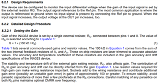
    In general, if you have multiple stages of op amp gain circuit, you want to place higher gain stage in the front. In this case, you may do 2000*20 or 1000*40. INA333 IA datasheet is recommended to have gain of 1000, but since your differential input signal is so small, I think that gain of 2000 may be acceptable. 

    Gain=4000 may be too high for the application. I need more data to support the gain configuration. I will ask our test engineer, if they have any experiences in configure such settings in the IA, since you max. signal is only 0.05mV (0.05mV*4000 = 200mV). Technically, it may be feasible, but normally we do not recommend high gains of IA. In addition, Rg value will be smaller and parasitic resistance and capacitance on a PCB may play a role in creating additional unwanted errors. Also, the op amp stability may become a factor. 


    With 0-10g force measurement, your system has to be calibrated prior to operate every time. So the two point calibration will linearize the measurement range. If you are able to calibrate a 3rd data point (say in the mid point at 5g or even check for the 3rd reference point in the mid range) you will have very accurate system, and will be able to minimize any errors in the system and/or operating environment vs. time. 

    BTW, LM7705 is switched capacitor voltage inverter with a fixed -0.23 negative voltage regulator with input supply voltage from 3V to 5.5Vdc. 

    If you have additional questions, please let me know. 

    Best,

    Raymond 

  • Hi Rodrigo,

    What is the rational for choosing gains of 2000 * 20 on the INA and 2nd stage, vs. say 1000 * 40 or 4000 * 10? Is there a sweet spot that will minimize noise or other considerations?

    As the bandwidth is no issue here I would go for 1000 x 40.

    But the actual limit of total gain will be given by the appearance of most odd offset voltages anyway: You need enough headroom to prevent the stages from going into clipping before you can adjust the offset voltage in the microcontroller. So I would try to find out the absolute worst case offset voltage in your application and then choose the gain in such a way that clipping is impossible to occur.

    The manual offset calibration with the cermet-trimmer can help to ease the situation. The cermet-trimmer playing the role of a fire extinguisher Relaxed

    Kai