This thread has been locked.

If you have a related question, please click the "Ask a related question" button in the top right corner. The newly created question will be automatically linked to this question.

LMH6515: Output attenuation issue

Part Number: LMH6515
Other Parts Discussed in Thread: ALLIGATOR

Hi,

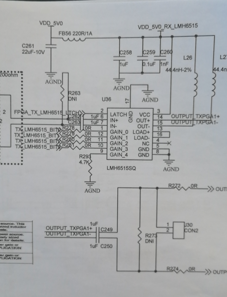
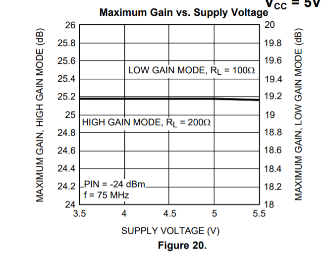
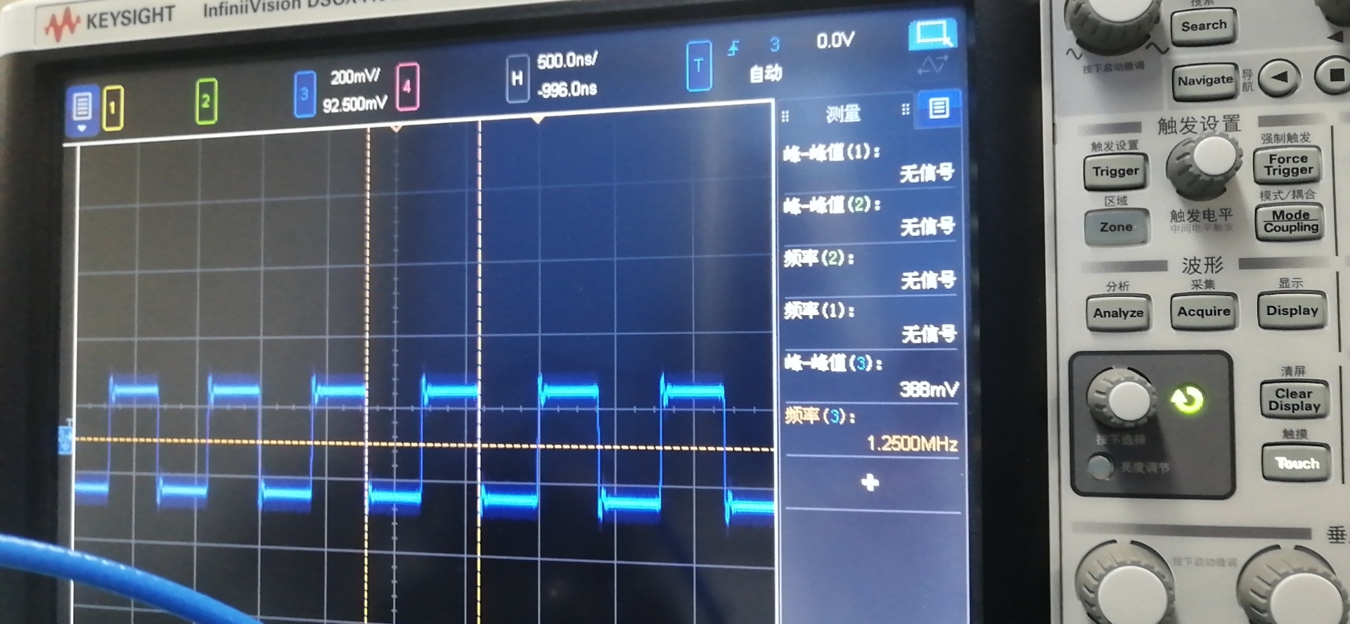
Please find the schematic for LMH6515 in the below. The input signal is 500mVpp at 25Mhz, but the output level is just 80mVpp. Could you please help review the schematic and give your suggestions? Thanks.

  • Hello Tess,

    I will take a look and see what I can find.  I might ask for more information should the need arise.  You may also email me (via the directory) if you to reach me outside the forum.

    Best,

    Alec Saebeler

  • Hello again Tess,

    For the application of this circuit here, what signal is being sent from the FPGA to LMH6515 latch pin?  When the LATCH signal is set low, the gain switches/pins immediately and directly affect the output.  If those gain values are set to low gain,  LMH6515 will be at minimum gain (which is quite low due to the shorting together of the load pins).  This could explain the low output signal.  However, I am considering other options as well.  

    Also, with your input 500mVPP signal, can I confirm the signal frequency is 25MHz?

    If possible, could you share a complete schematic and/or any additional information the customer has provided?  You may send these via my email (my last name is pretty unique) if public disclosure on the forum is not recommended.

    Please let me know of anything else you would like me to be aware of.

    Best,

    Alec

  • Hi Alec,

    Thanks for your prompt reply.  The frequency is 25Mhz. Latch is provided at 3.3V high state.  

    Could you please guide for the gain setting? The load is shorted for 200ohm low gain mode. I have two questions here:

    1. The output is attenuated about 6 times(~80mVpp) from the input(500mVpp).  And I find the minimum gain is about -7.7dB (max) which I think the output should large than 500mVPP*0.412(-7.7dB) =206mV.  ICC current measured is 105mA. The test condition is that we left the GAIN _0-5 pin float and give high logic at LATCH. Do you have any test result to compare for this condition?
    2. High gain mode and low gain mode setting?  Why the RL in the picture below is between 100ohm and 200ohm, and I suppose this should be 400ohm and 200ohm.


  • Hi Tess,

    Thank you for all the additional information!  I am working on getting insight on test results to help my understanding of how the LMH6515 has behaved in our tests.  I am working on some ideas about potential causes.  Also, I will consider the values and measurement you provided and work on answering your questions.

    Best,

    Alec

  •  Hi Alec,

    I'm really looking forward to your reply. Thanks.

  • Hello Tess,

    I talked through some ideas with my team and I have three potential options for you to consider.  I hope these help and give a good starting point for a solution.

    1) During your tests, you have had the digital gain pins floated, or left floating.  The LMH6515 does not mention functionality when the pins are left in this uncertain state.  Try testing the part/circuit while setting the gain pins, or have them set before the latch occurs.  

    2) The LMH6515 does not have input or output impedances like a typical op-amp.  The input impedance may not be as high, nor the output impedance as low as those of a typical amplifier.  Could you provide the input and output impedances of your source and measurement devices?  There may be attenuation occurring outside of the gain-setting performance of the device.

    3) Examining the 'Application Information' section of the datasheet, please consider Figure 42.  This figure, as well as surrounding text, discuss and display the relationship between bandwidth and chosen inductor values.  As you can see, the gain will attenuate the signal at a 25MHz for the inductors you are using.  Rather than swap out your inductors, you should try operating your circuit at a higher frequency (using Figure 42 for cross-referencing gain/inductor behavior).  If your circuit performs closer to your expectations, you may be filtering out some of your 25MHz signal with the 44nH inductors.  Larger inductors may perform better and be an eventual design recommendation.

    Please read through and take a look at these ideas.  Once you have the input & output impedances for the source/measurement devices, or have more questions, please let me know.  I believe these options should give you more tests/ideas for solving this problem.

    Best,

    Alec

  • Hi Alec,

    Thanks for your response. The issue is resolved with larger inductor value 6.8uH. And digital gain pins floated situation the gain tested is -15dB(about 5.6 times attenuation vs the input). When pulling the GAIN_4 high, the signal gain approximate 0dB. 

  • Hi Alec,

    The test for 1.25Mhz seems not pass. Please refer to the input and output screenshots below:

    Input signal:

    Output signal:

    The load inductance is 22uH and we also tried 6.8uH, the output still has issue.

    Could you please take a look and give some advice? Thanks.

  • Hello Tess,

    I will take a look and consult with my team.  Did your earlier attenuated output also have this distortion?  Or is this waveform distortion new since we reviewed the design and made some changes?

    You mentioned you have already checked how varying the load inductance would affect the circuit at 1.25MHz.  I will work on some other possible causes/advice.

    Best,

    Alec

  • Hi Alec, 

    This is waveform distortion new after some changes on design since we reviewed the design.

  • Hi Tess,

    Your 1.25MHz input may be filtered by the high-pass filter present in the LMH6515.  The part has datasheet specs for 35MHz and I believe you mentioned it worked at your bandwidth of 25MHz.  Could you confirm your load and bandwidth requirements (such as typically 25MHz, but down to 1.25MHz)?  There may be another VGA which could be better suited to your lower bandwidth use.  Are there additional specs the customer needs which informed the choice of VGA?

    Also, if you want to stick with the LMH6515, I can help with using an output filter.

    I am also curious about the ~7V output value you are getting from this part.  You are using a 5V supply, perhaps there is some resonance/inductance complicating your output.  What level of output voltage (based on set gain, etc) are you expecting from this design?

    Please let me know your output load (I assume this is an FPGA pin?).  I do see from an above thread you are using the LMH6515 in 200Ohm low gain mode.

    If you could also provide some context for why a 1.25MHz test was performed, I would appreciate it as well.

    Thank you for your patience and detailed responses Tess.

    Best,

    Alec

  • Hi Alec,

    The design is aimed to achieve bandwidth 0-66MHz output. The load is ADC. The gain range  is -10 to 25dB. And output target to be Vpp=2.2V.  And we would like to stay with LMH6515 solution.

    I have attached the initial post for device selection post here for your reference: e2e.ti.com/.../3551235

  • Hi Tess,

    Thank you for your response.  I will take a look and give you an update soon.

    Best,

    Alec

  • Hi Tess,

    I had a quick thought today: what probe type/setup are you using to measure your output signal?  The large ~7 volt output could be introduced by an inductive GND alligator clip.  If you have not tried it yet, you could use a 'tip & barrel' probe setup to minimize probe inductance and perhaps achieve a better output result.

    This may not be something that helps or you may have already considered and tested this.  I am also continuing to pursue additional ideas regarding your customer's issue.

    Best,

    Alec