Dear Specialists,
My customer is considering LMC6442 and has a question.
I would be grateful if you could advise.
---
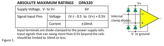
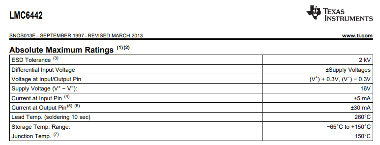
Regarding LMC6422
(1) When a non operating voltage (0V to 1.8V) is applied between the V + and V- terminals,
Voltage is applied to Input pins ± IN_A, ± IN_B or Output pins OUT_A, OUT_B,
Does current flow through the V + or V- terminals ?
(2) Does current flow when the maximum rating of the input / output terminals is within the range of (V +) + 0.3V and (V-) -0.3V?
(3)Would you please have a diagram of the internal circuit configuration if possible?
---
I appreciate your great help in advance.
Best regards,
Shinichi