This thread has been locked.

If you have a related question, please click the "Ask a related question" button in the top right corner. The newly created question will be automatically linked to this question.

TLV2172: Damage analysis

Part Number: TLV2172
Other Parts Discussed in Thread: TINA-TI

Hi team,

1. Customer feedback is as follows:

The customer produced a batch of products (317pcs) and reported a total of 5 sets of equipment with performance failure. One of them reported a performance failure when it was powered on at room temperature, and the other 4 reported a performance failure when it was taken out of the high temperature box after it was aged at 50 ℃ for 2 hours.

According to the disassembly analysis, TLV2172 failed. After TLV2172 was replaced, the failure was removed and the function returned to normal.

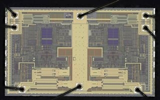
2、The customer entrusts the testing organization to analyze the fault TLV2172 . Through the analysis of ultrasonic and X-ray, the following phenomena are found in the faulty 3pcs

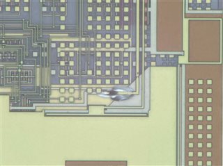
(1) There is an unknown mark in the inner layer

(2) Bottom X-ray found layered 

1 is normal, 2, 3 is bad

(3)Corrosion and burning marks are found on the tendon after opening

(4)All the opening products are from the same batch

The customer purchased TLV2172IDGKR through 云汉芯城, and the order number of 云汉芯城 purchased from TI: T01057115, T01033854.

Please help to analyze the causes of the above results

  • Hi Amy,

    to me this looks like a classic ESD damage.

    Kai

  • Hey Amy, 

    Can you provide the customer schematic and tests performed between the removal of the esd bag until the time the damage occurs?

    All the best,
    Carolina

  • Hi Kai,

    Thank you for your answer.

    Could you tell me how to judge the damage caused by ESD and what is the basis? Because we have to explain to the customer. I know this question is a bit unreasonable or unprofessional and hard to answer, but it's a customer's question. We have to explain it to the customer. so please bear with us.

  • Hey Kai, 

    Did you mean ESD or EOS? 

    All the best,
    Carolina

  • Hi Caro,

    could be both. What do you think?

    But looks more like arcing due to ESD :-)

    Kai

  • Hello Kai and Amy, 

    I am not sure what ESD damage looks like on a die level. 
    I have in the past seen damage to the ESD cells through Electrical over-stress (EOS). 

    If the customer is observing proper ESD precautions, I would think this is related to EOS, which is why I had asked about the customer's application.

    Also if you would like, we have TIPL videos that explain ESD and EOS.

    All the best,
    Carolina

  • According to the location of the damage in the picture, could you tell me which pin to pin damage it is

  • Hey Amy, 

    I have acquired within to see exactly where the damage is located. As an applications engineer, I usually bench verify the failure -- I haven't had to analyze which type of failure/location. 

    However, I can tell you that sometimes the damage location can be random. I think it would be best if we were to look at the application to make sure that no limits are being surpassed. 

    Additionally, could you provide what percentage of devices have experienced this damage? Was it fixed with an ABA test? 

    All the best,
    Carolina 

  • Hi Carolina,

    The customer said that because the company's patent was involved, the schematic could not be provided completely. The figure below is the application circuit of TLV2172IDGKR.

    In addition, the customer did ESD test according to your judgment. But we find that it doesn't match what you think is possible. The customer has done three ESD tests, 4KV, 6kV, 8Kv, to verify the damage to the chip, but the opening result is completely different from the damage phenomenon on the previous products. The location caused by ESD is random, but the damage phenomenon is consistent. The following figure is one of the ESD open pictures.

    According to the phenomenon of open film damage, can the possibility of ESD be ruled out?

    In addition, the customer also conducted three EOS tests: the VCC was supplied with 40-60v power for Impact pressure test, which was also inconsistent with what you thought. The opening diagram of one of them is as follows

    According to the phenomenon of open film damage, can the possibility of EOS be ruled out?

    In addition, could it be caused by latch-up effect?

    Looking forward to your reply as soon as possible

  • Hi Amy,

    I have seen many times damage from a discharging cap during power-down. Assume the supply voltage is decreasing faster than the cap would need to be discharged. Then a current is flowing into the input of OPAmp:

    There are many workarounds for this case:

    1. Keep the capacitance small enough so that the time constant formed by the resistive voltage divider and the cap is lower than the time needed for the supply voltage to fall down.

    2. Insert a current limiting resistor (red) of some kOhms.

    3. Mount a supply decoupling cap which is some orders of magnitude higher than the cap at the input and allow a "natural" power down (no short to signal ground or another sharp power down). If a sharp power down cannot be avoided, insert a discharge current limiting resistor in front of the big decoupling cap.

    Having said all this, a 2n7 cap should not be able to store enouge energy to damage the input of OPAmp. But who knows...

    Another reason for a weirdly appearing damage of OPAmp is oscillation. I have seen many OPAmps which got damaged just because of oscillation. And I ask myself whether your circuit has a stability issue. Well, what I'm not enjoing to see the feedback resistors 100R and especially 10k. Together with the input capacitance of OPAmp they provide a phase lag and erode the phase margin. Best basis for oscillation...

    So, finally, I think the whole circuit should undergo a careful revision.

    Kai

  • Hey Amy, 

    TIPL has a number of stability videos to introduce the topic linked here:https://training.ti.com/ti-precision-labs-op-amps-stability-introduction 


    Additionally, Bruce Trump has a few blog posts regarding stability, I find this one to be particularly useful: https://e2e.ti.com/blogs_/archives/b/thesignal/posts/taming-oscillations-the-capacitive-load-problem 
    The attached PowerPoint (in the blog post) is a very at-length descriptor on how to see if the customer's circuit is experiencing stability issues/how to fix them through TINA-TI. 

    It is recommend that each individual op amp is tested for stability. 

    All the best,
    Carolina

  • Thank you very much for your analysis and detailed reply. We will do experiments to investigate the above reasons.

    In addition, can the location of the damage be confirmed?

    Another fact is that the damage of three abnormal devices is found at the same location, and the damage phenomenon is consistent, which is obviously not random, so you need to help answer

  • Hey Amy, 

    We are not allowed to confirm the location of the damage. This information is confidential to our design.

    The team has some questions for the customer:

    1. Does the customer know which channel being damaged?
    2. Are there any connectors on the output? if there are then they probably need to add some ESD protection.
    3. Is there spikes on the power supply or differences in the GND plane? Is there any high current switching on the board?

    The inputs look like they have current limiting resistors so the damage probably isn’t coming from the input unless its coming through the cap on the non-inverting input.

    All the best,
    Carolina

  • Amy,

    Just looking at the metal pattern suggest that pin 7 was the entry point for the EOS. 

  • So Amy, what is connected to pin 7?

    Kai

  • 1. We can't confirm which channel is damaged. We provide the opening picture, which is the reason why we hope you can help us confirm through the picture. What we can confirm is that the impedance value between VCC and GND is abnormal, which is only 470 Ω, and the normal value is about 226k. Because other pin values have been opened, they cannot be retested.

    2. The output end is a pad connected with an induction coil. The output is protected by TVS and current limiting resistor.

    3. The power supply is 5V provided by LDO. At present, there is no peak in the graph captured by oscilloscope.

    There is a high current relay on the circuit board, but it belongs to the strong current part and is completely isolated from the op amp power supply circuit.

  • Hi Amy,

    an induction coil at the output? This explains it all !

    Add these two Schottky diodes as shown below:

    The BAT54S should work. Or take a slightly stronger one.

    If the LDO cannot absorb flowing back currents, add a series diode into the supply line of OPAmp and don't forget to mount the TVS at the top of above schematic.

    Kai